Modern MEMS magnetic sensors can provide a high resolution readout of the local magnetic field. Most commonly they are used for navigation, in combination with other sensors or by themselves as a compass. There is a lot of information lost if the magnetic sensor output is converted to one of 4 or 8 cardinal directions. To better understand the shape and variation of the magnetic field in my surroundings, I wanted to make a device which would visually indicate the 3D direction and magnitude of the sensed magnetic field. A few approaches are possible:
I picked the last approach, because it would be visually appealing and operationally flexibile in that it can be used as a hand-held sensor for immediate indication in any environment with no prior calibration or set-up required (other than calibration of the sensor itself). It would be relatively easy to 3D print a spherical surface with mathematically defined locations for indicator LEDs, which would be mapped in software to certain 3D angles and turned on or off correspondingly. The magnetic field sensor can be located inside the sphere so the indication is spatially accurate. This design would be "proper 3D" in that it is a spherical surface without easily defined planes or reference features, so it would be an interesting challenge to make in CAD.
At first I was thinking of using two-color bidirectional LEDs, with one color indicating the front end of the vector, and another color indicating the back end. Then each LED would have to be individually controlled, and eventually an array would need to be implemented such as charlieplexing. This would make the design rigid to changing the number and locations of LEDs, and furthermore means only one set of LEDs may be powered on at once. There are also quite inexpensive RGB individually addressable LEDs, with which an indefinitely long chain could be programmed with only one daisy-chained data line. This avoids the complexity of arraying LEDs for multiplexing, and allows many LEDs to light up in many colors, therefore more intricate display algorithms can be used. The RGB LEDs would seem better in all aspects, but they have one drawback - approximately 1 mA current draw per LED even when idle. With approximately 200 LEDs for reasonable 3D angle resolution, this would mean a minimum of 200 mA, which is challenging in terms of battery longevity, trace width, and generating a magnetic field in close proximity to the sensor which would interfere with the measurement.
I simulated the magnetic field impact of 100 mA current carrying traces using FEMM 4.2. The results suggested that minimal external field would be achieved by having identically sized traces with the supply and return traces in very close proximity to each other (of course). The closest they can be arranged is on opposite sides of a 2-layer flexible PCB which in this case would be 0.1 mm thick, and the magnetic field impact at the sensor location would be under 0.5 mG. This makes the RGB LED approach more attractive, but there is one more factor which settles the decision in their favor. Unlike individually lit LEDs which would show an angle quantized to the LED locations, a surface of individually addressable LEDs can be programmed with a color gradient to allow for visual interpolation between the LED locations, effectively increasing the display angular resolution.
The approach then would be to use a chain of RGB LEDs arranged on a flexible circuit board of a particular pattern, which can be folded around a 3D printed spherical surface to make a spherical display. The firmware would have a list of the LED 3D locations and would set the color of each LED accordingly.
When making a spherical display, where should the pixels be located? It is desired to arrange them in a uniform manner so the display looks similar from any angle, and so that any vector from the origin may be drawn with reasonable resolution. The article Distributing Points on the Sphere, 1 discusses some methods.
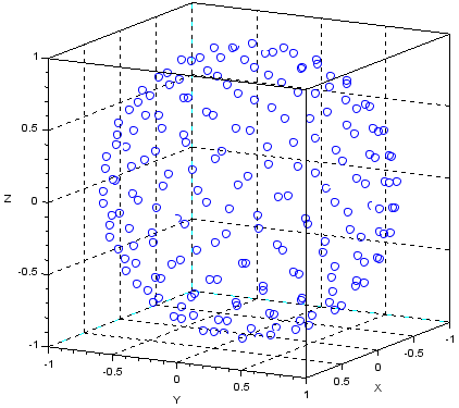
A distribution of 201 points on a sphere using the golden ratio method.
A distribution based on irrational intervals in latitude and longitude (Scilab code file) makes for a "natural" looking sphere, however the poles appear different from the equator, there are no defined antipodes of each point (to properly show front and back of a vector), and there is no way to separate the sphere into smaller identical parts for ease of fabrication (other than a symmetry line across the equator).
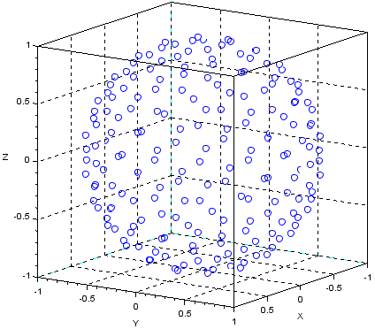
A distribution of 194 points on a sphere by splitting an octahedron along faces - edges - edges.
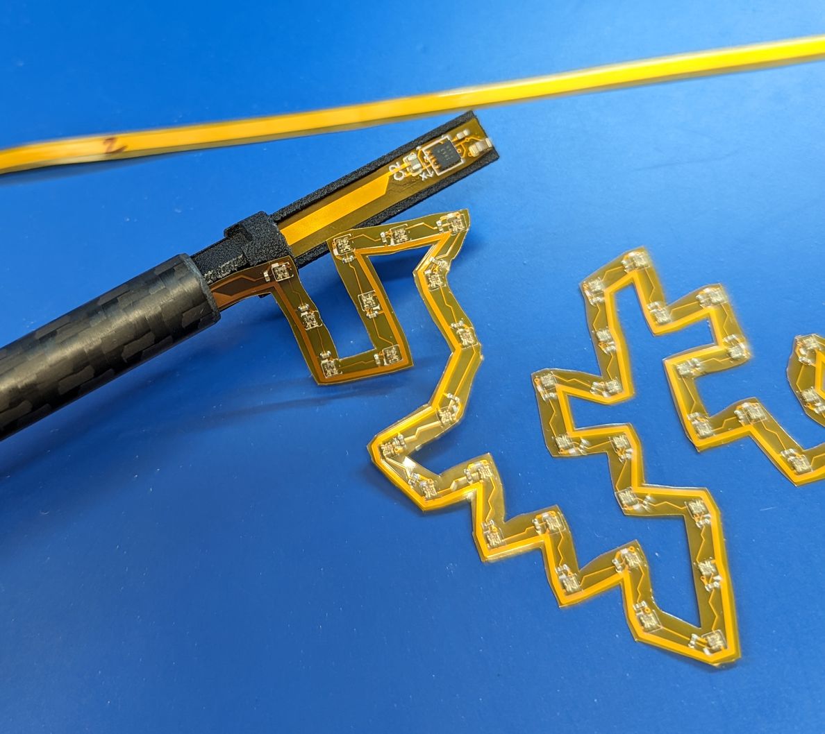
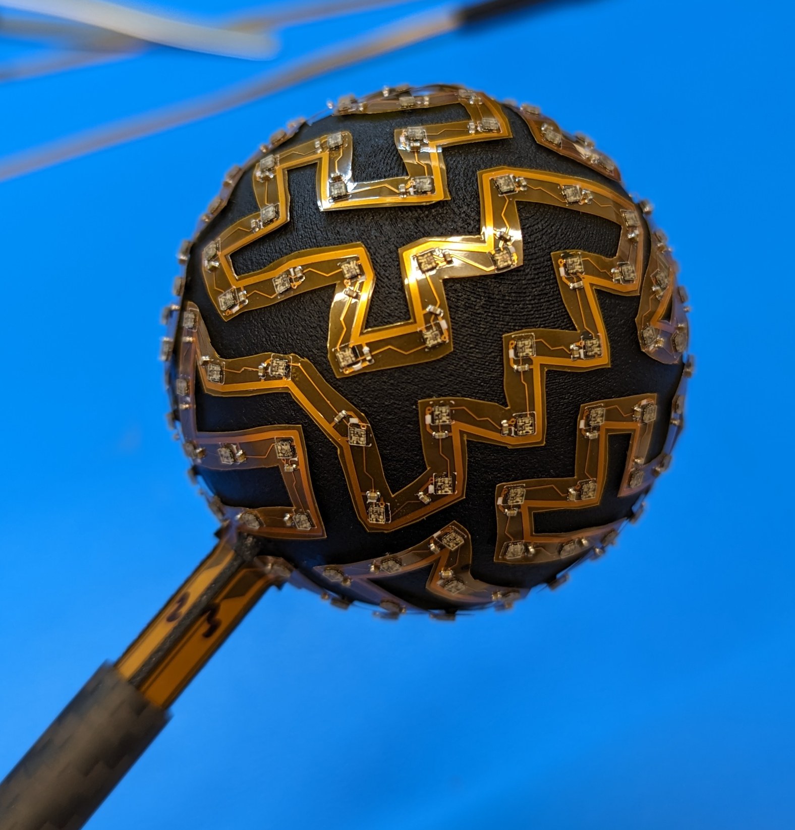
Another approach starts with a regular polyhedron such as an octahedron or icosahedron, and then splits these into more finely spaced points. The splitting may be on triangular faces using the face midpoint (Scilab code file), or on edges using the edge midpoint (Scilab code file). The number of points resulting from the splitting is a limited set, and the split result is not guaranteed to maintain uniformity on the sphere surface, so I pick a split routine that gives nearly 200 points and looks uniform. Trying a few different starting shapes and splitting types, I found that starting with an octahedron, then splitting once on faces and twice on edges gives a visually appealing distribution without large gaps or differences in point spacing, with a total of 194 points (Scilab code file). In this case each point has an exact antipode and there is octahedral symmetry so the sphere may be split into 8, 6, 4, or 2 nearly-identical sections. I divide the 194 points into 4 sections or slices around the Z axis, so that 4 identical (with the exception of the poles) LED flex PCB shapes may be used to cover the sphere. This is easier to manufacture due to a smaller PCB size and trace width required, and also means the current in each PCB is reduced along with its magnetic field impact. (Also having 4 PCBs means the data is sent out more quickly since 4 data lines are in parallel, requiring about 1.5 ms overall to refresh the LED array, but this rate is not a limiting factor in this design.)
The geometry here is a sphere and there are current-carrying traces at the surface of the sphere. With a sensor at the center of the sphere and a constant current through a loop, if the loop is going around the equator, the circle is large (magnetic field at center reduced) but its center is close to the sensor; if the loop is going around one of the poles, the circle is small (magnetic field at center increased) but its center is far from the sensor. On the sphere surface, to minimize the magnetic field at the center, would it be preferred to have high curvature or low curvature paths for the current flow? A calculation using a simple offset current loop approximation suggests that high curvature is better. Therefore instead of spiral-like paths for the LED chain, zig-zag paths are chosen. Another advantage to the zig-zag path is that it can better accomodate non-idealities in point spacing during assembly, because the angular bends may slightly flex to result in linear expansion or contraction at further away points, and there are more angular bends present compared to a spiral path.
Once we have established the locations of the LEDs on the sphere surface, it is necessary to find out the 2D shape of a flexible circuit board that could wrap around the sphere and place the LEDs in the specified locations. The LEDs are arranged in a chain, so the path of the flex PCB should traverse the sphere surface from one LED to another. To have a sheet with one axis of curvature pass through two points on a sphere surface, the sheet must bend in the same manner as a circle of the sphere's diameter (and centered on the sphere's center) that passes through the two points, or a "great circle". Then the unwrapped distance or great-circle distance between the two points is the length of the arc along the sphere's external projection onto a plane through the sphere's center which contains the two points. More simply, it is the angle in radians between the 3D vectors defined by the two points, multiplied by the sphere radius.
//from math.stackexchange.com/questions/1143354/
//theta=acos(sum(p1.*p2)); //angle between unit vectors - not good for small angles
theta=2*atan(norm(p1-p2),norm(p1+p2)); //better for small angles
We also need to determine the angle by which to turn in the 2D plane so it will wrap around the sphere to reach the subsequent point. Here we have an intersection of two great circles through a central point, and if we locally project to a plane, the angle within the plane is the same as the angle between the normal vectors of the two great circles. Further, these normal vectors will always be perpendicular to the normal of the projected plane when the projected plane is tangent to the sphere at the circles' intersection. The rotation therefore must be about the normal vector of the projected plane. A formula using the dot product and the determinant gives the angle with a consistent sign corresponding to clockwise or counter-clockwise turns.
n0=cross(p0,p1); //previous plane normal of arc
n1=cross(p1,p2); //next plane normal of arc
n0=n0/norm(n0); //make unit vectors
n1=n1/norm(n1);
cc=sum(n0.*n1); //cosine of angle
//formula from stackoverflow.com/questions/14066933
//ss=n0(1)*n1(2)*p1(3)+n1(1)*p1(2)*n0(3)+p1(1)*n0(2)*n1(3)-p1(1)*n1(2)*n0(3)-n0(1)*p1(2)*n1(3)-n1(1)*n0(2)*p1(3); //sine of angle
nd=cross(n0,n1);
ss=sum(p1.*nd);
theta=atan(ss,cc); //negative values means turning clockwise in plane, zero = straight line
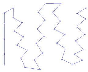
In the 2D unwrapped plane, we start at (0,0) heading in the direction (0,1), then for each point on the sphere we turn by the calculated angle and move forward by the calculated distance. This gives the unwrapped path (Scilab code). To verify the approach, I 3D printed a sphere surface with the calculated points marked, then printed out multiple path patterns on paper and attempted to wrap the sphere. I generated the surface in CAD by starting with a sphere primitive, importing a list of calculated points, and then defining a tangent plane and sketch at each point, a tedious process that made me better appreciate the abilities of more programmatic modeling (such as OpenSCAD or Grasshopper / Rhino, although I did not use either). With 194 points that are symmetrically arranged, I would consider this design towards the end of what I would want to do with a CAD GUI, as beyond this it becomes easier to write a custom routine to generate the desired 3D mesh than to keep track of the multitude of points, sketches, and reference geometry.
The 3D printing test was successful, as all the tested path profiles when printed on paper and cut out along the path would be capable of wrapping around the sphere surface and lining up with the point locations, so I used the same method to specify the order and locations of LEDs in the 2D flex PCB file. It was helpful to have the 3D printed surface in hand when laying out the path for the LED chain, because it was difficult to visualize the points even with computer renderings; I used small pieces of painter's tape to mark out the path and make small adjustments to avoid sharp angles (difficult to bend) and spiraling structures (magnetic effect), then I entered this path as a sequence of point indices to generate the layout of the flex PCB.
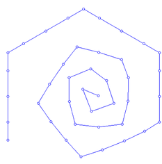
Spiral and zig-zag paths computed in the 2D plane.
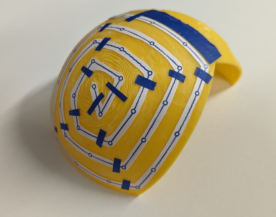
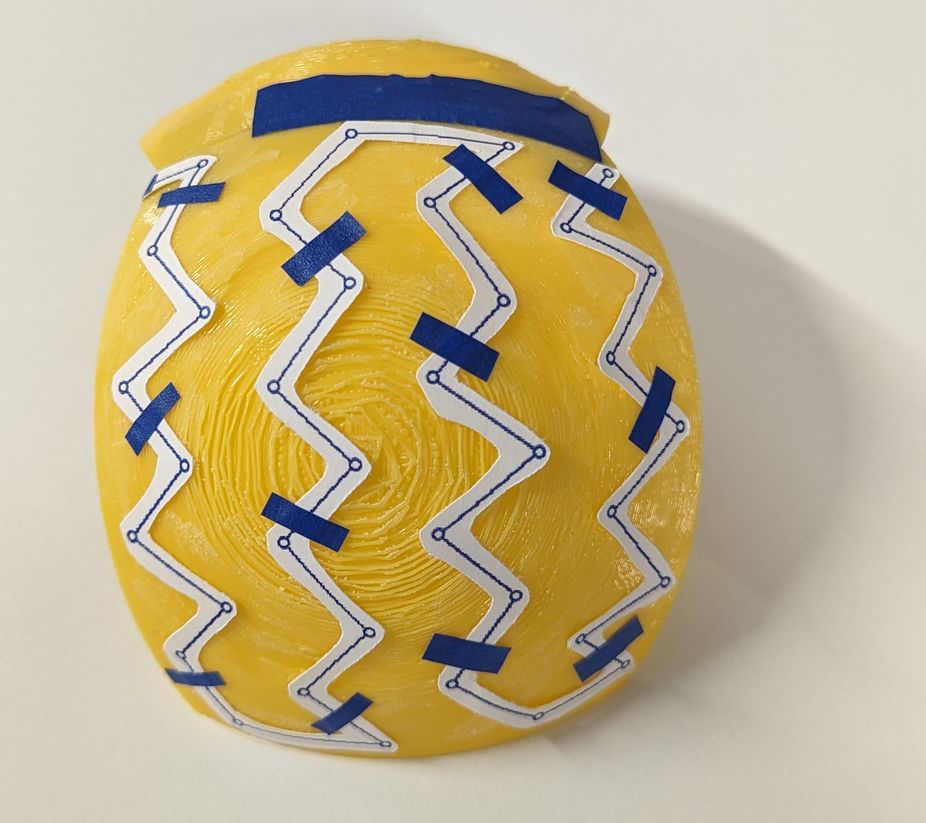
A 3D printed partial sphere shell along with a printed shape on a piece of paper are used to validate the sphere path unwrapping approach. In the 3D printed shape design, small holes are located at designated points, and the circle symbols on the cut-out piece of paper line up directly over the holes when the length scales are correctly defined. The spiral path and zig-zag path both work as expected.
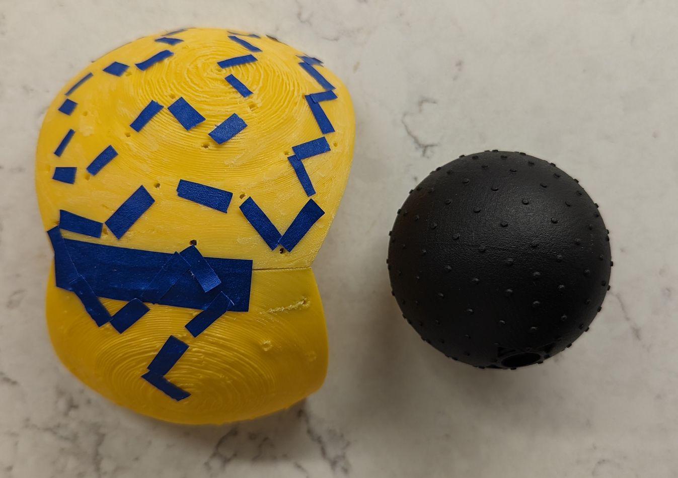
The final version of the path is physically simulated with painter's tape. The relative sizes of the prototype sphere shell and the final indicator sphere may be compared (the diameter of the latter is under 0.5 x that of the former).
The path that has been laid out on the physical model is traced back in software by finding the corresponding sequence of projected point indices. The indices in turn are mapped to 3D coordinates of each point.
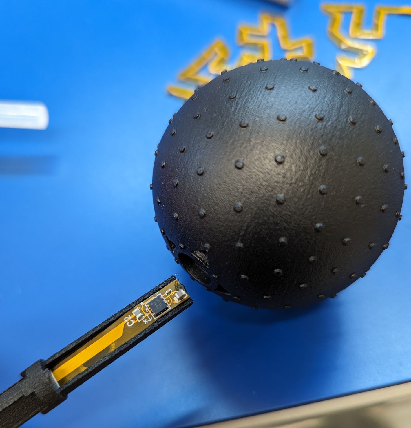
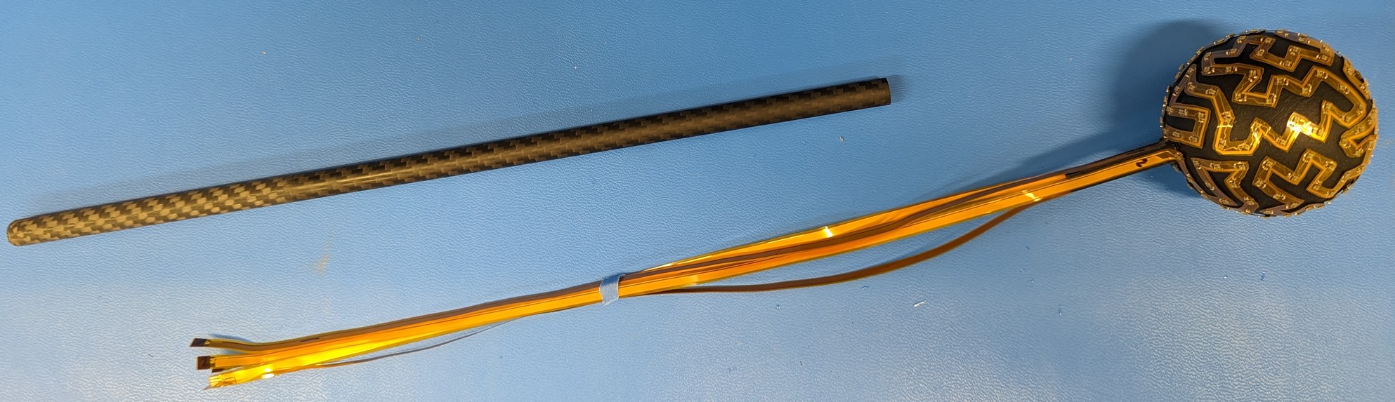
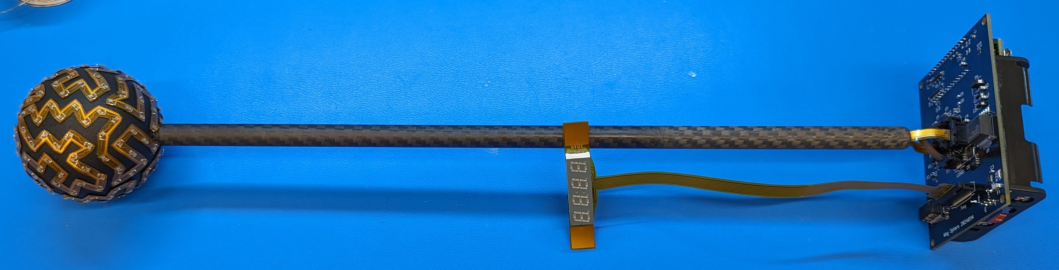
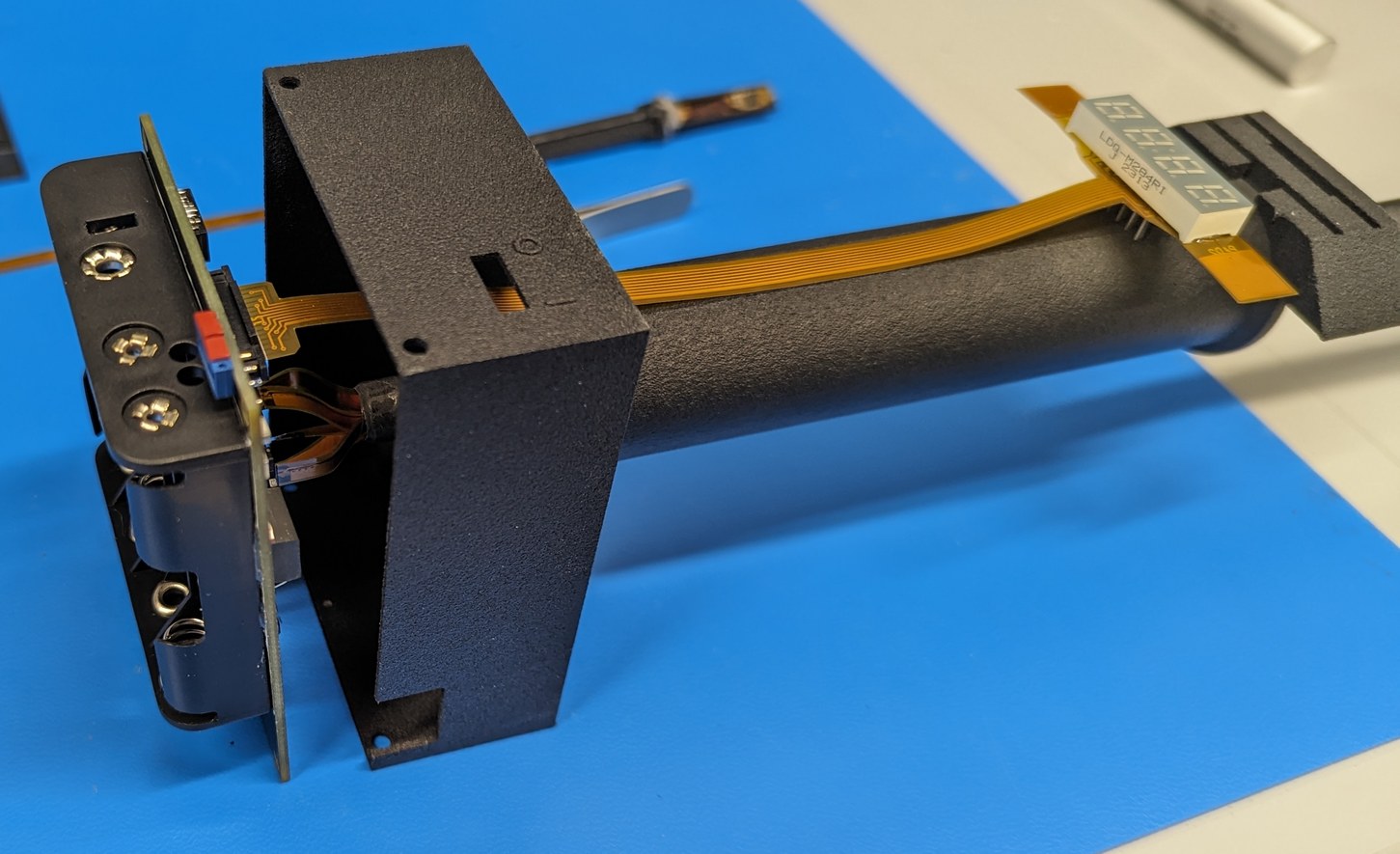
The magnetic sensor would be located inside the 3D printed sphere, so I decided to place it on a flex PCB which could be glued to a holder that centers the sensor relative to the sphere surface. The main benefit is that the flex PCB could connect to a FPC connector on the main (rigid) PCB, meaning there would be no need to manually solder wires, and the width of the connectors could be smaller than what would be required for manual soldering. Everything would look neat and compact, and disconnecting various components for troubleshooting would be easy. To maintain this benefit, I added a long "tail" on the end of the main flex PCB, such that the handle of the device could be some 300 mm away from the display sphere. This distance would improve visibility of the sphere, and would place batteries and other potentially magnetizable components far away from the sensor.
The spherical display probably will not give a good indication of field magnitude, since brightness is not easy to visually evaluate. There may be ways to achieve this, such as a ring normal to the magnetic field vector, or time-based animations, however it is desirable to have some quantitative measure, as well as general auxiliary outputs for the device (such as battery voltage and calibration status). For this, a 4 digit 7-segment LED display is used. Another flex PCB is used for the 7-segment display, to allow it to be positioned on top of the device's handle while maintaining the benefit of a compact connection to the main PCB. To either side of the 7-segment display, capacitive touch areas are added on the flex PCB, to act as buttons for selecting the operational mode. This uses the built-in capacitance sensing functionality (touch sensing input module) of the MKL26Z64VFT4 MCU on the Teensy LC (which I showed previously could be used for a capacitive DDR pad).
The device will operate from 4 AA batteries to supply the necessary current at 5 V. Because the batteries may drain to nearly 5 V (and lower), especially if using NiMH rechargeable ones, a low dropout regulator (with 0.2 V dropout) is used. If all LEDs are set to the highest brightness simultaneously, the power draw would be near 3 A (these rather severe restrictions leave few contenders for the LP3873). With realistic battery resistance of 0.4 ohm for 4 AA batteries in series, the battery voltage will drop below 5.2 V at 3 A; nonetheless using components that can handle the full current means I could use a different type of battery in the future, or perhaps the voltage drop would be tolerable because the LEDs continue to operate below 5 V. It is unlikely that I would ever set all LEDs to the highest brightness in regular operation (that's 15 W electrical power and uncomfortably bright to look at directly), so being near the dropout limit in this way is not too concerning.
The power requirements here end up similar to the acoustic field camera despite the differences in physical extent (in fact this device is capable of drawing a slightly higher current than the AFC's receiver board). Thus I use a similar approach of a INA232 voltage and current meter with a 0.03 ohm shunt resistor, a 3 A SMD fuse, a filter based on a 1.5 uH SMD inductor and 1000 ohm ferrite beads and 10 uF and 1 uF capacitors, and a SIP32509DT load switch to programmatically turn the LEDs off if necessary. A 5 V Zener diode prevents overvoltage on the 5 V rail and an ESD protective diode is connected to the touch button traces. The circuit architecture is designed to be safe with any readily achievable configuration of power inputs and outputs, such as being powered by Teensy LC USB, powered by both USB and battery, powered by battery only, and having the LED 5V rail power on or off in any of these cases. In particular this is done by having a Schottky diode on the 5 V line leading into the Teensy so that a USB connection cannot back-feed into the battery, and by using the TXU0104 to interface with 5 V ICs, where the TXU0104 is specified for operation with the supply voltage on either side of its translation boundary present or absent.
The MMC5983MA Anisotropic Magneto-Resistive sensor is used, which has nominal measuring range of +-8 G and 18 bits resolution, which is 0.061 mG per LSB. The earth's magnetic field is on the order of 500 mG so this sensor will be able to indicate small changes in the field direction. The achievable resolution is tested by recording 10000 consecutive samples at 100 sa/s data rate. (More details on this approach are given in the ADC Quantization article.) Communication is over a dedicated I2C bus (since the sensor is over 300 mm away) with 3.3 Kohm pull-up resistors. When starting continuous acquisition, the reading changes by a few mG every 10 seconds over about 5 minutes, probably due to temperature rise when the sensor is active. A linear fit is used to subtract out this change, and a histogram of the spread of raw values is plotted. This shows the noise is normally distributed, with 2*sigma of {7, 12, 16} LSB on the {X, Y, Z} axes respectively, which is +-{0.43, 0.73, 0.98} mG.
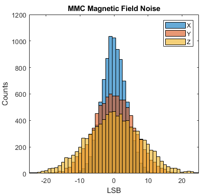
A histogram of one particular MMC5983MA variation in bit reading over time on each axis, after subtracting a linear trend.
Since 100 sa/s is too fast of an update rate for recognition on a visual display, we may average it to improve the result. With 8 samples per average, we can update the display at 12.5 Hz, and achieve 2*sigma of +-{0.15, 0.26, 0.35} mG. This averaging is expected to have below 0.01 x impact at the approximately 1 Hz bandwidth variations in the magnetic field that should be visualized when moving the sphere for a nice dynamic indication. To avoid the visual noise of a rapidly changing 0.1 mG digit, the 7-segment display shows integer values of the field in mG. The 4-digit range of 0000 to 9999 if interpreted in mG matches well with the magnetic sensor's limit of 8000 mG.
After obtaining a magnetic field reading and correcting for sensor offset, the total magnetic field strength in mG is shown on the 7-segment LED display (LDQ-M284RI). There are 4 digits, which share 8 cathode pins (one for each segment + dot), and each have one of 4 anode pins. This makes for a total of 12 pins for 32 LEDs, compared to just 4 data lines for 194x3 LEDs on the spherical indicator. However, the neediness of the 7-segment display doesn't end there. Originally I intended to drive it by connecting the 4 digit pins through a TXU0104 voltage translator, which applies 5 V instead of the Teensy's 3.3 V and outputs a higher current of 12 mA per pin. The voltage drop of the LED and current-limiting resistors on each segment pin allow the other side of the display to be connected directly to the Teensy. This is not an ideal configuration due to the 12 mA current limit of the TXU0104 and due to the potential to expose Teensy pins to 5 V. More pressingly, resistors of 2 Kohm per segment were chosen to not exceed 12 mA per digit when all 8 segments are powered on, however with the resulting low current the display was unreadably dim. An approximately 2 mA current is a decent value for a discrete indicator LED, however here the digits are displayed one at a time, therefore any single digit is on for 1/4 of the total time, and there is a corresponding 4-fold reduction in brightness. The diffuser further reduces apparent brightness. Since I had already soldered in the 2 Kohm resistors, it was easier to add some extra 511 ohm resistors in parallel, which gave 6.7 mA per segment. At this current, the display was readable, but not very bright. If all eight segments are on (53.6 mA), this exceeds the TXU0104 output current rating by a factor of 4.4, which is not a good design.
Thus I remade the main PCB, so that a MOSFET is used on each of the 12 pins going to the 7-segment display. The p-type high side MOSFETs (PJC7409) are driven by the 5 V outputs of the TXU0104 (inverted, as 0 V at the gate allows digit current to flow), while the n-type low side MOSFETs (PJC7410) are driven by the 3.3 V Teensy pins directly (inverted, as 3.3 V at the gate allows segment current to flow). This is a better design overall because it completely isolates the voltage and current paths of the 7-segment display from the Teensy and from the TXU0104, however it is annoying that this took more design effort than the individually addressable LED chain. For anyone considering using a traditional 7-segment display like this, I would rather recommend making a pseudo 7-segment display out of individually addressable LEDs and a 3D printed baffle + diffuser structure; it would be a lot easier to drive (in terms of pins, ICs, and CPU resources required) and would offer more flexibility in terms of displayed brightness and color.
In the new board revision I used a lower resistance of 90 ohms per segment, which allows for about 25 mA per segment and 200 mA per digit when all segments are powered on, within each MOSFET's 500 mA rating. The digits are now easily readable. The average current requirement of the 7-segment display is not negligible at around 100 mA. The firmware code is littered with calls to update the state of pins driving the 7-segment display, because the 4 digits have to be cycled through rapidly to not appear flashing at a 0.25 x duty cycle; 10 ms per digit is already not acceptable due to the digits appearing to flash, and 2 ms per digit seems like a decent value - but then the pins must be updated every 2 ms with some regularity to avoid brightness differences between digits. Once again, individually addressable LEDs would be a better choice as they can be set once and remain at their defined brightness level without host processor intervention, as all the needed PWM timing is done locally.
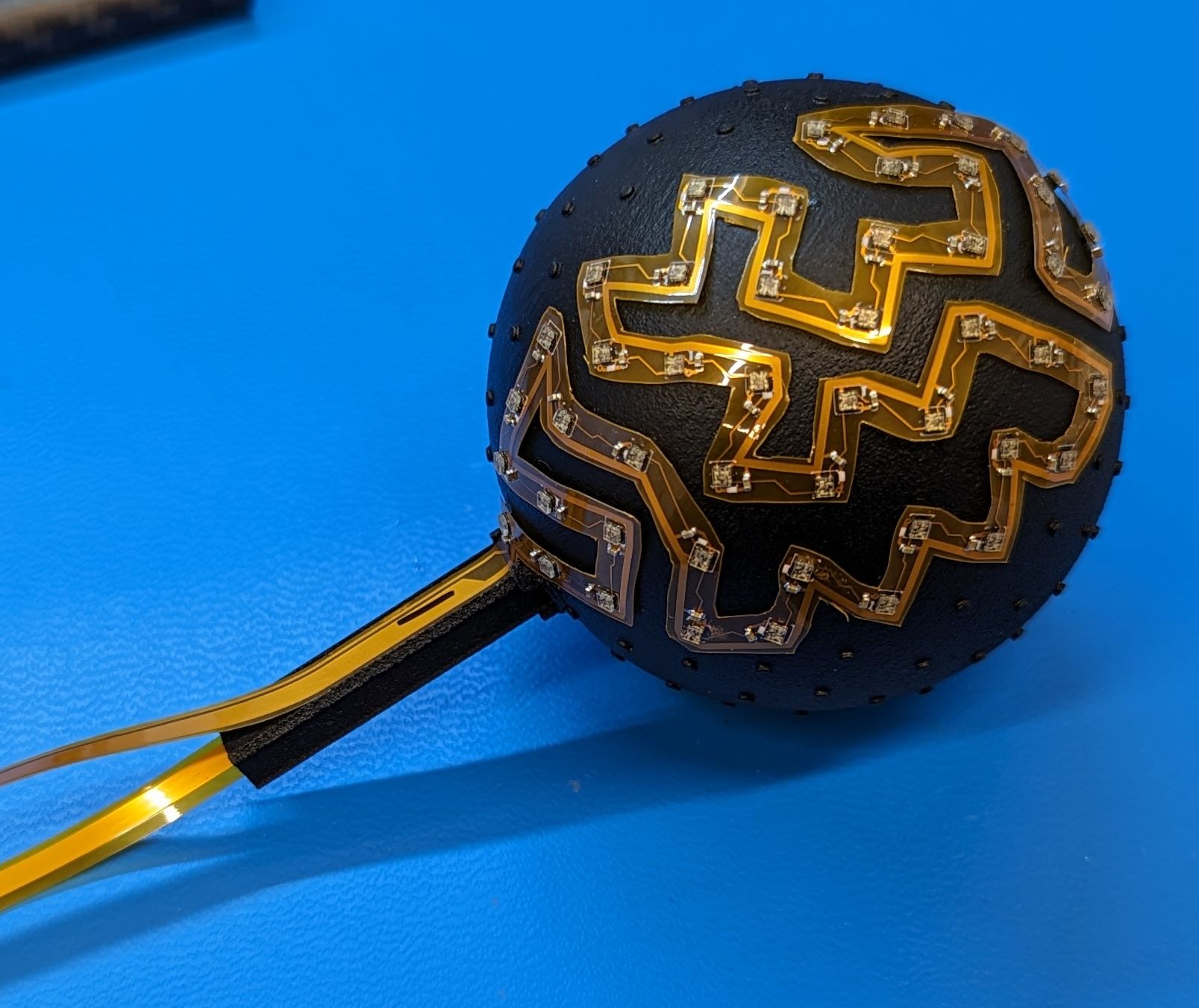
There are 4 LED strips that are wrapped around the sphere. Each LED on each strip is mapped to a 3D location on a spherical surface as defined above (Scilab code) and these locations are stored in the firmware code and used to calculate the LED brightness to render a 3D shape. The LEDs are driven through a TXU0104, which translates between the Teensy's 3.3 V and the LED stip's 5 V. The strips are identical except for the last LED, which is installed on only one of the strips and removed on the other 3, because this LED is at the Z+ pole point where all the strips intersect. (This would prove to be a not great choice, because it is difficult to cut the flex pcb while guaranteeing that the 0 V and 5 V traces, separated by only 0.1 mm on the inner layer, do not form a short circuit. I would recommend designing a dedicated cut point where the traces are well separated, or designing different PCB versions with and without the last LED.)
To output the digital signal from the Teensy I use a modified OctoWS2811 library (included in the firmware linked below), which is changed so that 4 pins are driven instead of 8. This is done by keeping the same DMA approach writing to the GPIO output port register, except instead of SET - WRITE - CLEAR which updates all 8 pins in the middle step of assigning a value, I use SET - TOGGLE - CLEAR, which can update any 1 to 8 pins (hard-coded to 4 in this project); all other pins remain available for other uses. This requires a minor adjustment to invert the desired output values since they act as a flag on the toggle register, so a 0 output value is achieved by writing a 1 to toggle after a known set operation; the inversion is done when moving the pixel data from the drawing buffer to the frame buffer. Looking at an oscilloscope trace with the library running on the Teensy LC, I found a timing error on the first pulse sent out, which is present in the original library as well. Between how the compiler optimizes the code, and how the Teensy LC handles writes to FTM2_xx registers, the timing of the final parts of the OctoWS2811::show() function was not straightforward - in fact the first rising edge had already been output when the timer was still being set up. I found that the first pulse length could be maintained within datasheet specifications for the LEDs (300 ns for 0, 600 ns for 1), though still not as consistent as the following pulses, by changing the order in which the DMAs are enabled and calling FTM2_CNT=0 after every instruction to prevent the pulse from ending prematurely.
But this was not the end of the story. When testing the LED string, I found that pulses {811, 812, 817, 818} (zero-based) were sporadically lengthened or offset (while the period remained unaffected), which caused LEDs 33 and 34 to sporadically light up in blue or green. With 1.25 us per pulse, this happened from 1013 us to 1023 us after the start of the pulse sequence. In the calling code, I had a delay(1) immediately after leds.show(), which accounts for the 1000 us. Something after the delay was causing the DMA timing to be perturbed. This turned out to be the touch controller; somehow starting a capacitance measurement by writing to TSI0_DATA caused jitter in the timing. Since the entire pulse sequence takes under 1.5 ms, I fixed this by using an elapsedMillis object to ensure that at least 2 ms have passed since the previous leds.show() call before the capacitance measurement would be started.
I worked on the main PCB, the LED array flex PCB, the 7-segment display flex PCB, the magnetic sensor flex PCB, and the PCB enclosure all at once, because the locations of connectors and the lengths of the flex PCB "tails" would all need to match the final component locations in the enclosure and on the indicator sphere. The limits were determined by a 60 mm outer diameter for the sphere, a 430 mm total flex PCB height to keep the maufacturing cost reasonable, and a 300 mm separation between the magnetic sensor and the main board to reduce magnetic impact of the batteries (final separation was 370 mm).
For the LED array, after generating the unwrapped path with a scilab script as described above, in DipTrace I manually placed 49 LEDs at the 2D coordinates in a path that would cover one quadrant of the sphere. Then with some adjustment of the LED rotation angles to allow the data line to continue uninterrupted from one LED's DOUT to the next LED's DIN, and placement of one size 0402 (inch) 0.1 uF bypass capacitor per LED, the main part of the LED board was done. For the current carrying traces I used a polyline "shape" (in DipTrace lingo) instead of a "trace", because the shape is not subject to the same constraints as a trace in DipTrace, and it can be selected all at once. The latter aspect was used to create an exact copy on both top and bottom layers, such that the two traces are overlaid and have minimal magnetic field impact. When connecting to each LED, the bottom layer trace runs underneath the LED, to further help reduce the size of the current loop. The capacitors used have a soft termination which should help them handle the flexible nature of the PCB application. The LEDs, IN-PI15TAT5R5G5B, measure 1.5 mm by 1.5 mm, output up to 5 mA per each color, and use about 1 mA idle. These LEDs do not have a clear indication of the pin number or orientation when seen from above, there is only a tiny arrow marker on the underside (they are intended for machine placement and are pre-aligned in the tape direction, a thought occurs that many of the components used here could spend their entire existence in the industrial product realm without once being directly seen by a human), so I drew a sketch of how the LED looks like from above (the controller die, the 3 individual color LEDs, and the wire bonds between them are visible through the transparent plastic case), labeled with the pin numbers, to use as a visual reference for manually placing the LEDs. I ordered these LEDs as 10-packs from Adafruit instead of as a big batch because I thought it might save me the effort of dealing with SMD tape packaging, however this backfired as the 10-packs are simply cut pieces of tape and I now had to open each of the packs instead of just one tape section.
The other flex PCBs, for the magnetic sensor and for the 7-segment display, were fairly straightforward. I made a custom pattern to match a 4-pin and a 15-pin 1 mm pitch connector, the 15-pin for the 7-segment display, and the 4-pin for all others. This pattern included a silckscreen layer to indicate where a stiffener should be placed. I combined the three flex PCB designs into one compact area which I ordered as one line item from PCBWay. I did not include any cutouts, with the idea that I would receive a rectangular piece containing all the designs and cut out each one myself. A benefit to this approach is that the otherwise irregular-shaped boards can be handled as one rectangular piece during component assembly and reflow soldering, and the cutting can be done afterwards. This resulted in the stiffeners being placed at odd points in the middle of the polyimide sheet, which the assemblers at PCBWay did not seem to mind.
I used a stencil to apply solder paste for the LED array board, and manually applied solder paste for the other boards. After placing the components, I used a very small temperature-controlled hot plate (Miniware MHP30) for the reflow operation: I lowered the flex board onto the hot plate, and slowly (about 5 mm/s) moved the board around until all the components were soldered on. Due to the flex board's low thermal mass and low thermal conductance (meaning I could hold it with bare hands for better control), this approach worked well. Further, due to the flex board's transparency, it was possible to optically inspect the components from underneath to ensure no solder bridges had occurred.
Using a hot plate to solder the magnetic sensor (left) and prototype LED array (right) (only containing the first 10 LEDs of the 49) flex PCBs.
The main (rigid) PCB was drawn up in the usual manner, it was a 2 layer board with all the SMD components on the top side, including the connectors for all the flex PCBs, and the through-hole battery holder, Teensy, and power switch all on the bottom side. The 4 AA battery holder, with a mechanical drawing in the datasheet that required a bit of deciphering and guesswork to figure out the locations and polarities of the through-hole pins relative to the outer rectangle of the case, would be held on by a layer of hot glue on the PCB surface under the holder (when properly melted and wetting both surfaces in a thin layer, hot glue forms a good bond, contrary to the general opinion that hot glue is weak and flimsy). The locations of the connectors were aligned with bolt holes on the corners of the main PCB, and referenced to the enclosure and main rod through which the flex PCB tails would pass: the tails would exit just above the connectors to minimize the bending and maximize the useful length of the flex PCBs. The location of the power switch was aligned with a corresponding hole in the enclosure, and the expected location of the Teensy USB connector was aligned with a cutout in the enclosure to allow for firmware reprogramming and debugging without removing the board from the enclosure. These mechanical aspects were verified by using the DipTrace 3D board preview feature and exporting the main board as a step file (using solid model files from the component manufacturers when available and custom ones when not) then importing this file into Fusion 360 where the 3D printed structures were designed. The packages for many standard SMD components were generated automatically so this process was much easier than I anticipated. The DipTrace files for this project (schematics and boards) may be downloaded here.
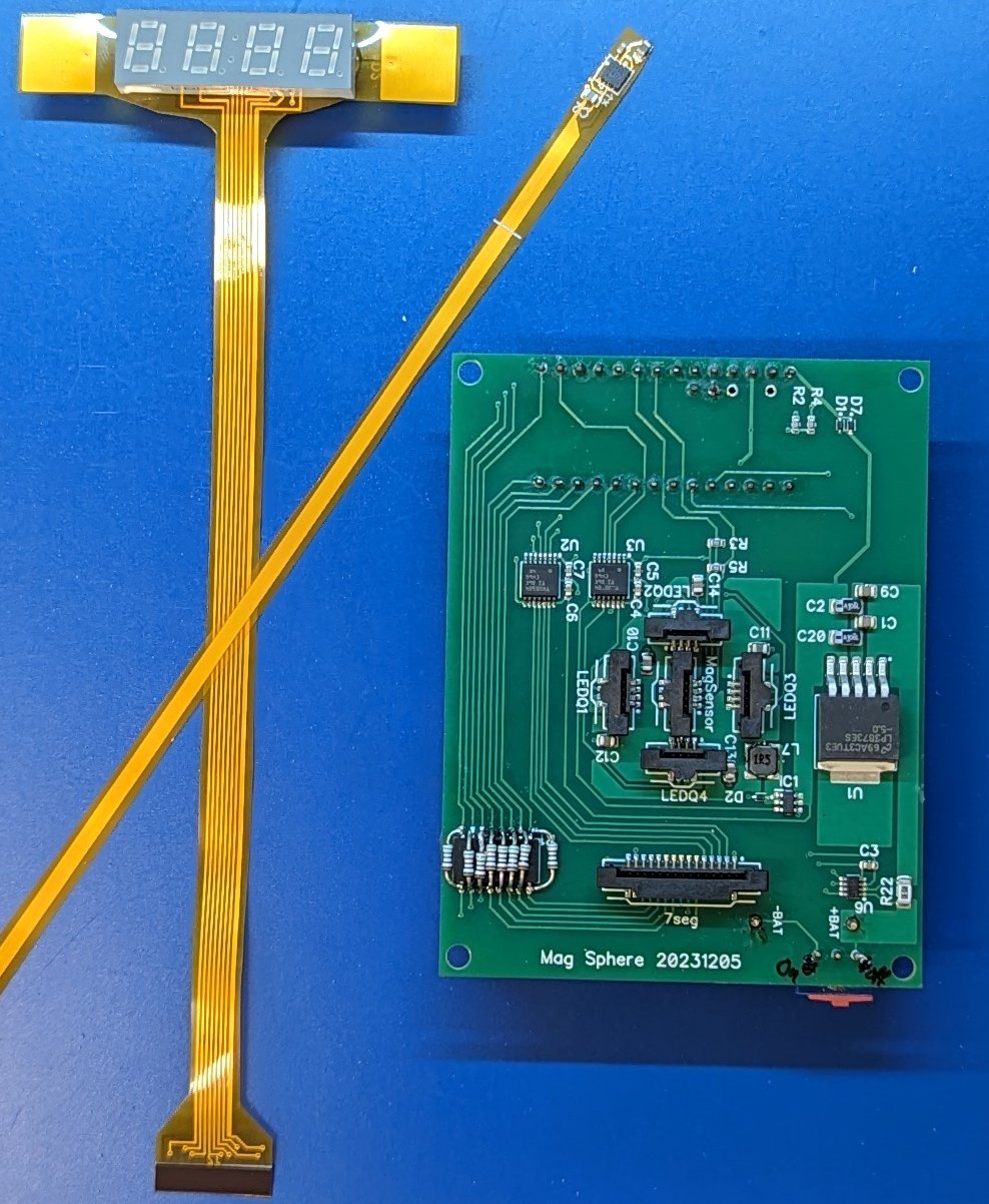
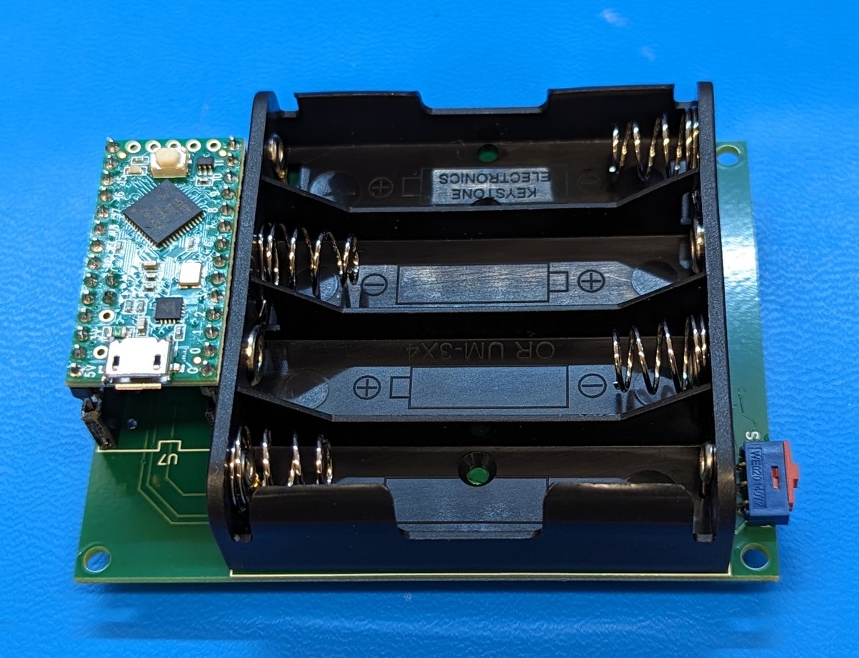
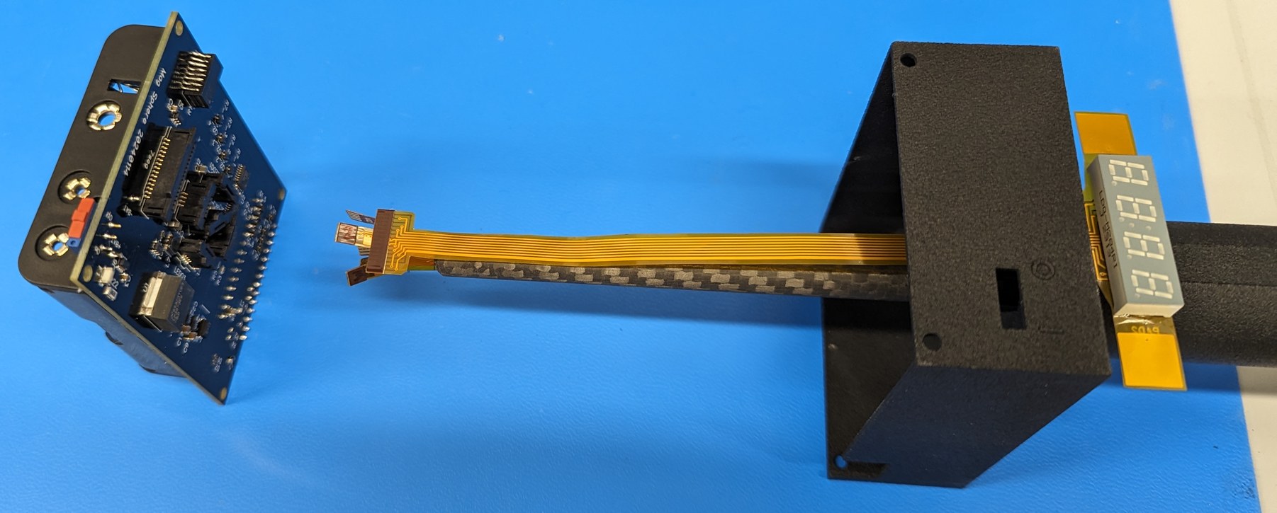
The main PCB and the flex PCBs for the magnetic sensor and the 7-segment display. On right, the underside of the main board is shown, with the battery holder and Teensy LC installed.
Once the soldering was completed, I tested the functionality of the individual flex PCBs with the main board. The magnetic sensor worked successfully (after enabling the second I2C port in one of the Teensy core files), and the 10-LED strip also worked successfully. The stiffener on the flex PCB end that would enter the connector was not perfectly aligned with the metal pads (due to a mistake I made in the DipTrace pattern) so on removing the end of the connector I could see that the divots made by the rigid connector were very close to the pad edges rather than centered, which is not great but the misalignment was within tolerance and the connection could still be made successfully. The 7-segment display was too dim which necessitated a redesign of the main board. I took this opportunity to correct a few other mistakes. The power switch would operate in the reverse manner of what was labeled (I originally made sure that the electrical side was routed correctly, double-checking my interpretation of pin names like "inverted shutdown", but I failed to notice that the switch itself was specified as reverse-acting). The connector for the magnetic sensor was aligned with the LED connectors but could be rotated by 45 degrees to fit in a more compact way. Protections for overcurrent and ESD were missing. The numbering of the LED connectors did not match the numbering of the sphere quadrants after assembly (this is a minor point as it's a one-line change in software, but as a matter of principle, it is good to practice consistency in labeling). On the 3D print side, I also made a mistake of using very small (1 mm long) notches to attach the indicator sphere onto the rod that would connect it to the rest of the assembly; I identified this as a failure point in the initial design but thought that a bit of glue would be adequate, and upon seeing the actual printed part it was clear that the glue would not be a reliable approach and that there was a means to extend the notches without affecting the path of the connectors in the rod. I sent the updated design files to PCBWay again and waited for the shipment. The 3D printed parts are also ordered on PCBWay, with HP MJF nylon, which gives a good print resolution, mechanical strength and flexibility, and a nice black surface finish.
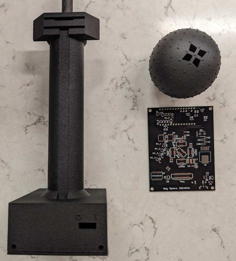
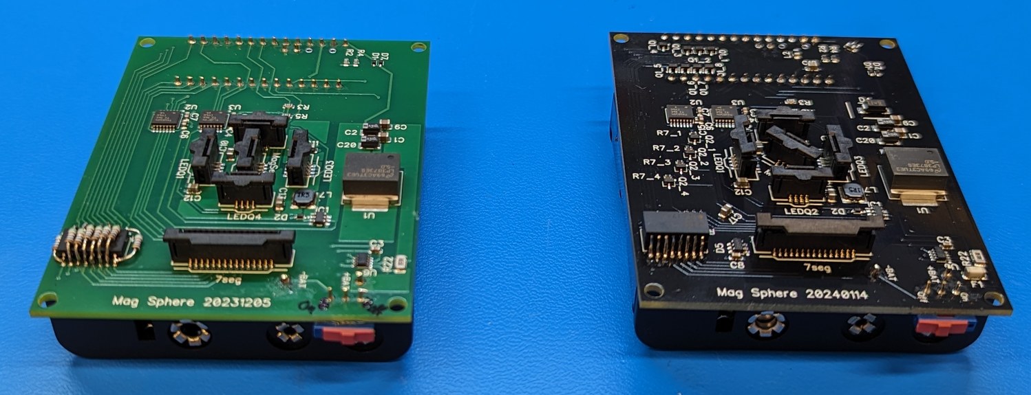
The second shipment of components along with the 3D printed indicator sphere. The main board has a black solder mask to match the color profile of the 3D printed parts (and the PCBWay reviewers placed the board product number inside the SMD resistor location so that it would not be visible once the resistor is placed, a nice touch). On right, a comparison of the previous and subsequent iterations of the main board after soldering.
In assembling the main board previously, I was hoping that the hot glue used to attach the battery holder to the board would be adequately dispensed from a hot glue gun, but it solidified too quickly resulting in a poor bond. On the updated version, I heated the entire board after SMD soldering, and applied hot glue, then placed the battery holder and pressed it down as the assembly cooled, resulting in a strong bond.
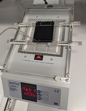
Using a PCB heater to heat the main board to slightly over 100 degC, in order to uniformly apply a layer of low melting point hot glue, for attaching the battery holder to the back of the board.
Having successfully tested the prototype 10-LED chain flex PCB, I assembled the 4 application PCBs with 49 (or 48) LEDs each and soldered with the hot plate as before. Then after visual inspection and electrical testing, I manually cut out the path of the LEDs.
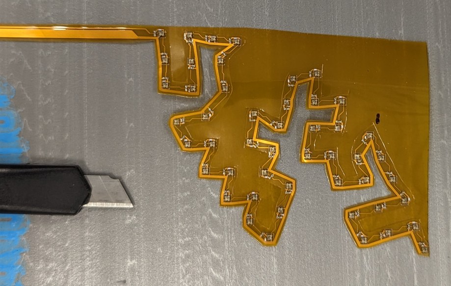
A knife is used to cut the path pattern in the LED array flex PCB placed on a foam backing.
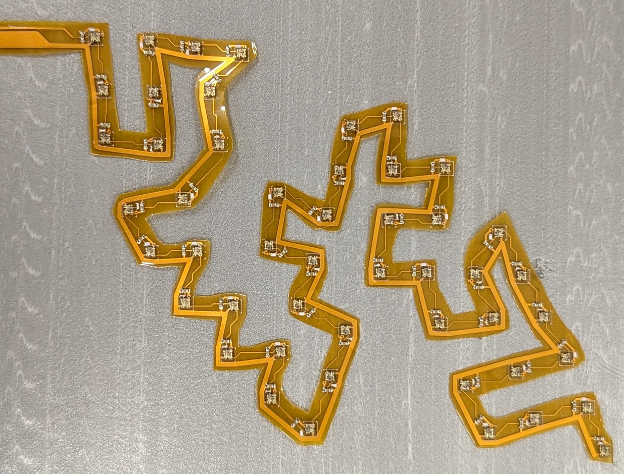
The 4 LED chains, one per quadrant of the indicator sphere, are soldered and cut out. The long tails of the flex PCBs allow the sphere to be located 340 mm above the main board.
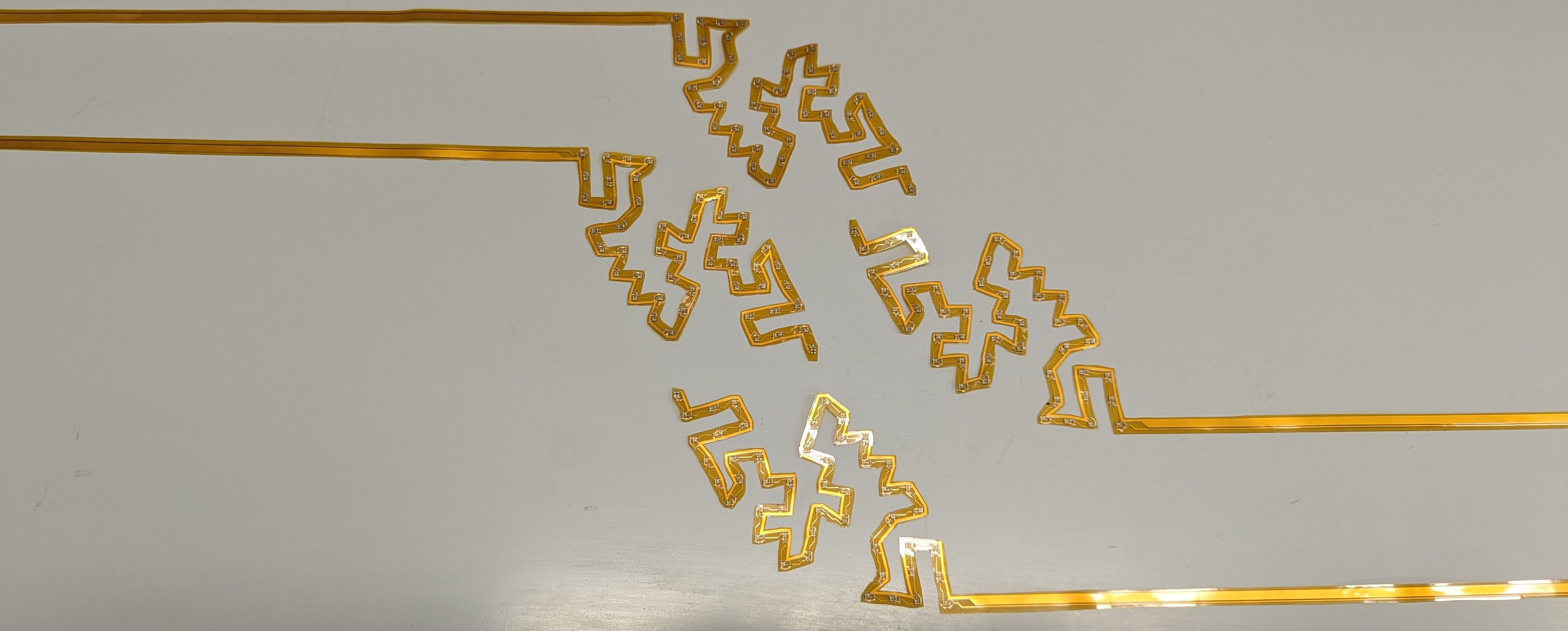
After cutting out the LED chains, they are tested with the new main board, and all function properly. The 7-segment display also works, but it would not be so easily tamed, requiring me to once again manually solder an extra parallel resistor chip to reach its specified operating current with a 90 ohm equivalent resistance.
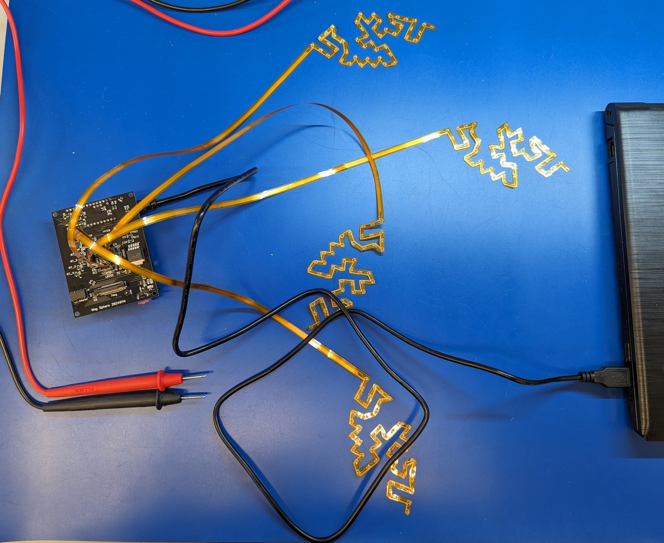
The test bench setup with voltmeter probes, connecting the 4 finished LED strips to the main board, in turn connected by USB to a laptop for debugging.
With all the boards tested, it is time to start assembling the structure, or in particular, gluing everything together. I use an "instant set" cyanoacrylate glue, which readily bonds the flex PCB to the 3D print surface. The bond is reasonably strong, yet because the flex PCB is smooth, the PCB may be peeled off later if it is necessary to re-position the bond, so it is not an indestructible permanent bond (at least within minutes after attachment). An initial fit test is carried out, because once the LEDs are glued on the sphere, it will not be possible to take the sphere back apart without undoing all the assembly progress to that point. After the gluing is complete, the sphere is attached to a carbon fiber rod (10 mm outer diameter) with the flex board tails enclosed inside the rod and connecting to the main board on the other end. Carbon fiber is chosen due to its strength and non-magnetic properties, and the rod has a matte finish to match the overall color scheme.
The fit of the flex PCBs and the 3D printed parts is confirmed. The widths of the tail sections must pass through corresponding slots into the carbon fiber rod and the sphere holder (which also holds the magnetic sensor at the sphere center) must attach to the sphere indicator.
Left, one of the sphere quadrant LED chains is glued. Small bumps on the 3D printed sphere indicate the LED locations; ~4 LEDs at a time are manually placed on top of the bumps and held in place while the glue sets. Small misalignments are absorbed by the flex PCB bending freely between the glued points.
This photo shows the full length of the flex PCB tails along with the carbon fiber rod through which they will pass once assembled.
This photo illustrates how the flex PCBs will be connected to the main board inside the handle of the device.
The carbon fiber rod caused slight difficulty in assembly. When designing the handle I wanted to avoid the frustration of the rod not fitting in the hole and made the hole 10.5 mm compared to the nominal 10 mm OD of the rod. Four bolts would be used to hold the rod, and in their locations I reduced the diameter back to 10 mm so the held sections would be tight against the rod. Then I thought 10.5 mm would be too loose and reduced the clearance to 10.2 mm. In the received part, of course, the rod was a very tight fit. Worse, the rod could be inserted with some force but then would become stuck and require substantially more force to try and remove (perhaps something to do with local deformation of the plastic pressed against the epoxy causing increased adhesion over time). I used pliers to remove the rod, which shattered one of the ends making it unusable; luckily I had a backup rod, unluckily this backup rod was an even worse fit. I used a round file to slightly enlarge the hole in the handle, and a flat file to slightly reduce the diameter of the rod, which helped a little bit. The intended assembly process involves sliding the rod all the way through the handle, connecting the flex PCBs, then sliding the rod back up until the main PCB is contained within the handle, and finally securing the rod in place. This requires the rod to slide freely through the handle. It appeared that the rod was not quite straight with regards to the handle, so if I were to expand the hole to allow the rod to slide freely during assembly, then it would not be held tightly once the assembly is finished, thus I had to take many small steps of slightly filing the hole and the rod, checking the fit, and repeating until the rod was held firmly but not stuck.
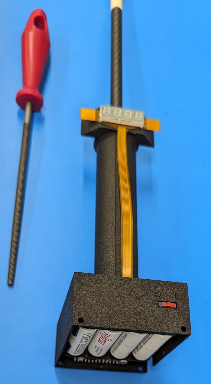
A round file is used to slightly enlarge the hole in the handle to allow the carbon fiber rod to pass through for assembly. The main board is shown installed with batteries in the bottom of the handle and the rod is coming out of the handle top.
I still stand by the logic of using a tight fit because it is easier to enlarge a hole than to reduce it, however for a high aspect ratio hole such as this (much deeper than diameter) the appropriate choice would have been to have the tight fit only for the first and last few mm of the hole (where the rod enters and exits the handle) while throughout most of the hole there would be adequate clearance for no interference at all. This would maintain the same pointing accuracy of the inserted rod, but would not be so sensitive to rod straightness, and in case of manual modification, the surfaces to modify would be small and easily accessible. Probably I didn't think of this originally because I am used to subtractive manufacturing where such a profile would require extra steps to produce.
With all that out of the way, it is time for final assembly! The sphere indicator is attached to the rod with a combination of hot glue and instant glue. Then the rod is inserted into the handle, and electrical connections are made. Then everything is bolted together using titanium M3 bolts (chosen to reduce magnetic impact).
Assembly step 1: The rod is pushed all the way through the handle, and the flex PCB connectors are secured on the main board.
Assembly step 2: The rod is pulled back out, and the main board is secured inside the handle.
The assembly process worked, although the location of the power switch meant that the main board had to be tilted in order to fit inside the handle and then tilted back to push the switch through the hole, which put an undesirable load on the flex PCB connections. Perhaps in another design the handle would have a cutout for the switch or the switch would be oriented differently, to allow the main board to be inserted without tilting.
On the surface, the role of the software is simple - read data from the magnetic sensor, process it, and display the result on the spherical indicator and 7-segment display. The details that make this more complex include capability to test each component over serial, cycling through a number of display and calibration modes with two touch buttons, regularly cycling through the 4 digits of the 7-segment display, and polling the sensor at a constant interval to keep its power consumption and temperature from fluctuating. Initially I tried to use multiple code files to keep the various hardware components separated, but it was not long before the annoyance of dealing with both *.c and *.h files overtook me and I returned back to the familiar approach of "one giant code file" (over 1000 lines). The main firmware file, along with the modified OctoWS2811 library, may be downloaded here. The firmware is compiled and loaded with the Teensyduino installation under the Arduino IDE.
I used a new (for me) pattern to cycle through the menus and submenus accessible with the touch buttons:
if(btn_event){
	menu++;
	btn_event=false;
}
switch(menu){
	default:
	menu=0;
	case 0:
	//do something for menu item 0
	break;
	case 1:
	//do something for menu item 1
	break;
}
The benefit of this approach is in simplifying the coding, because there is no need for the programmer to keep track of the total number of menu items. If there is a need to add more items, simply add more cases in the switch statement, and if there is a need to remove items, just remove the cases and renumber the other items. The menu variable will automatically be reset to zero when the valid cases are exceeded. The structure of the menu is then implicit in the structure of the code file. There might be even more clever ways to do this, such as a menu_temp--;if(menu_temp==0){} for each case, which would mean there is no need to either keep track of a total or to renumber cases when adding, removing, or changing order.
Rendering the scene for the spherical display can be math-intensive. I use floating point math, and originally had a call to the power function a=pow(b,c) in order to apply a non-linear scaling to the brightness of the LEDs. In addition to the 3D dot product call for each of the 193 LEDs (there is no LED where the rod connects to the sphere), the time to complete the function exceeded the 11 ms delay to request data from the magnetic sensor. This in turn caused a slower than expected poll rate, which reduced the sensor temperature, which caused the reading to be offset (by 5 mG to 10 mG) relative to a calibration done when the math computations were not slowing down the poll rate. To avoid this complication, I replaced the power calls by a cube a=b*b*b as this gave a visually similar effect and completed within the allotted time. (Remnants of the variables used for the power call may still be found in the code. There is in fact a missed opportunity to use antipodes to halve the calculation time.) While the calculation completed within 11 ms, the 7-segment display still had to be updated every 2 ms, so after every LED is calculated, a call is made to check whether the 7-segment display needs to be updated, and the update itself consists of 10 calls to digitalWriteFast(pin,val).
The handle is designed with a cutout that allows the USB cord to be connected to the Teensy for reprogramming. The cover, in the lower half of the photo, has a tab to fit this cutout so once installed the board is safely enclosed.
The USB serial port is monitored to allow checking and updating of some status parameters with a computer. Sensor calibration values may be saved to and read from EEPROM. Four visualization modes (at three brightness levels) are implemented:
In addition, there is a flashlight mode with white and colored static displays. When the main code was finished, there were still some 20 Kb of memory remaining, so I filled that with calculated coefficients of 35 spherical harmonics that could be visualized as a static display on the sphere.
The MMC5983MA sensor used here requires calibration for an accurate reading at the 1 mG level. In the lab, I had access to some large mu-metal shields, inside of which the magnetic field is below 1 mG, where I could measure a true zero reference. Without such shields, the calibration may be done manually by rotating the sensor about all three axes and finding the center of the point sphere made up of the sensor's measurements as it is rotated. However such a procedure must be done carefully, because even a few mm of lateral motion of the sensor's center point will cause a real change in the reading of a few mG, hence the rotation should be done with a purpose-built fixture that ensures the sensor remains centered in the same place. In fact such a fixture would provide a benefit over the shields, because the sensitivity of each axis could also be calibrated (this would be the width of the point sphere measured along each axis). In the absence of a good calibration, the spherical indicator appears "stuck", pointing in the same direction even when the device is rotated and moved about, because the uncalibrated offset is being displayed instead of the real underlying field. With proper calibration, the spherical indicator tracks a constant direction in space when the device is rotated, showing the real direction of the magnetic field.
The MMC5983MA datasheet describes the use of SET and RESET commands to calibrate a bridge offset. After a SET command, the sensor is magnetized in one direction, and after a RESET command the sensor is magnetized in the opposite direction. The offset remains constant, so assuming an underlying true value M, we can add the results of the two commands to obtain (M+Offset)+(-M+Offset)=2*Offset or we can subtract the results to obtain (M+Offset)-(-M+Offset)=2*M. Inside the magnetic shield, I found a non-zero Offset value and a non-zero M value (whereas the true M is expected to be zero, observed was on the order of 20 mG). The observed M value is used to calibrate the true zero for the sensor, and I found that this calibration coefficient does not change over time. The Offset value may be readily determined even without a magnetic shield (giving similar values inside or outside the shield), by using the addition formula above and keeping the sensor stationary during the measurement. This calibration coefficient was found to fluctuate over time (on the 2 mG per minute time scale), either due to sensor temperature changes or some non-ideal magnetization of the sensitive layer. However a quick SET+RESET measurement could be used to re-calculate the offset which would restore the initial performance. Both of the offsets apply in different amounts to all 3 axes, and their values may be stored to EEPROM to be used later. Axis sensitivity is not calibrated as I do not have a convenient way to do so, however a rough test of manually rotating the sensor about a constant center point shows that the magnitude of the field does not change by more than 2 mG, and the displayed field direction is stable in space, which is adequate for this project (again, much of this change in magnitude may be due to real difference in magnetic field from slightly moving the center of the sensing element). Within about 1 minute of a SET+RESET calibration, the field magnitude reading may be trusted to within 1 mG (though noting that there is no magnitude calibration applied). In more commonly encountered fields of over 100 mG magnitude, the angular accuracy of the measured vector is expected to be below the display resolution of the indicator sphere.
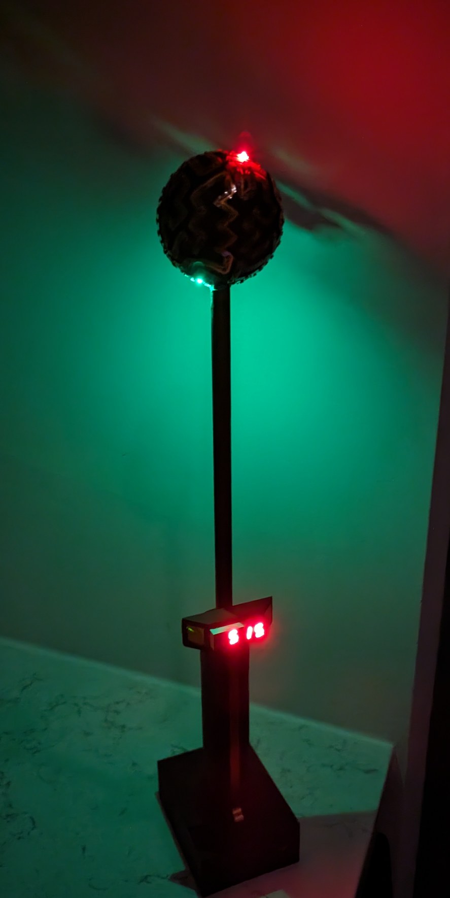
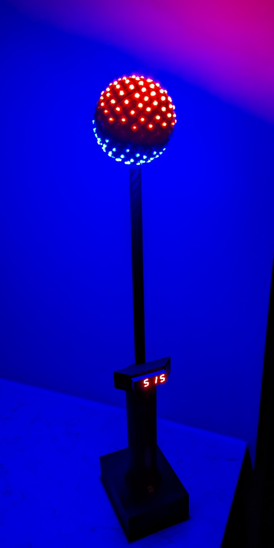
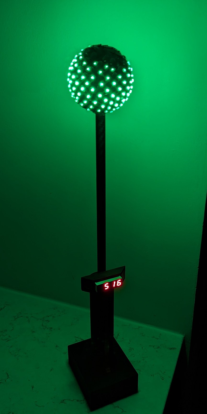
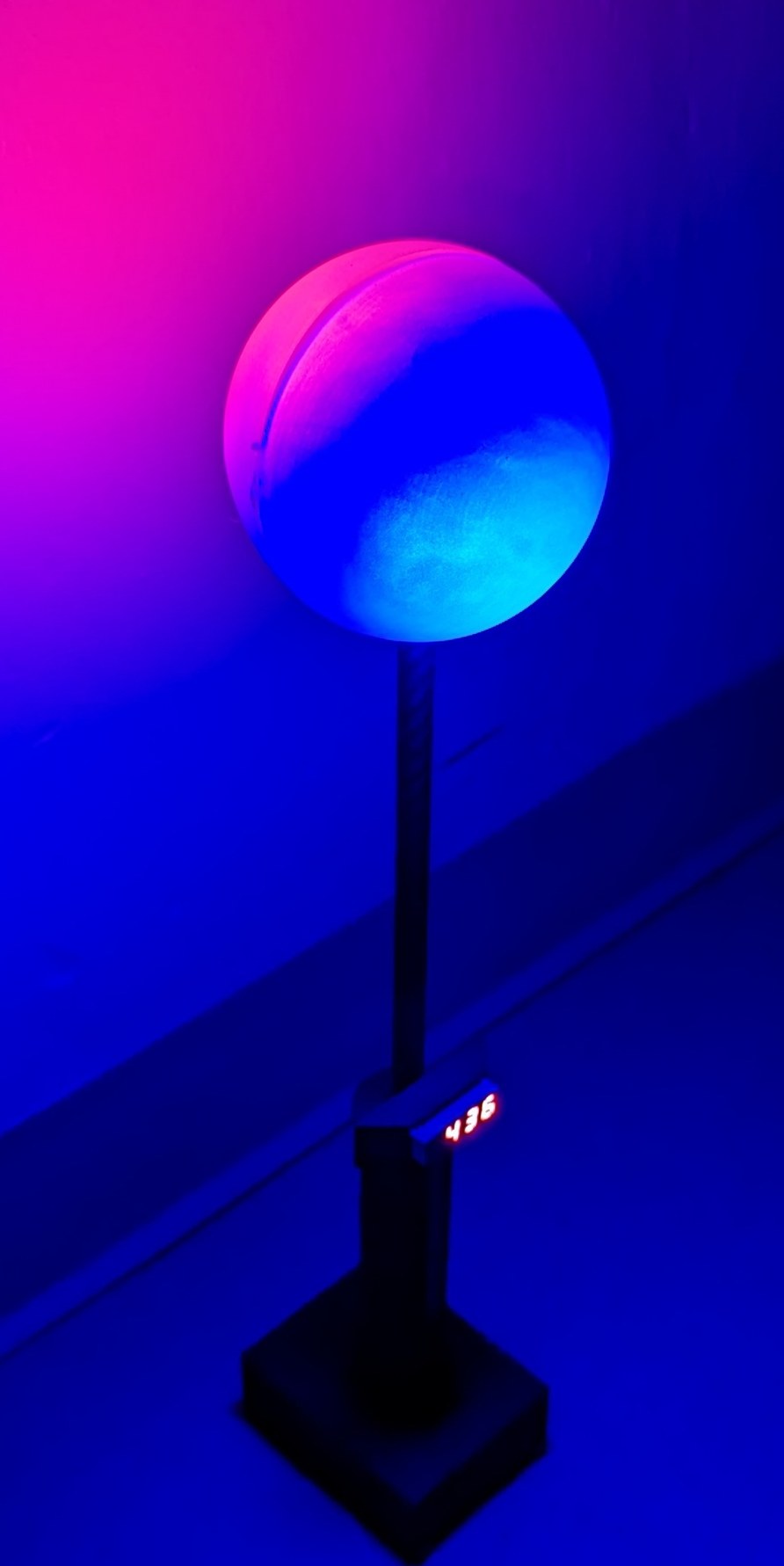
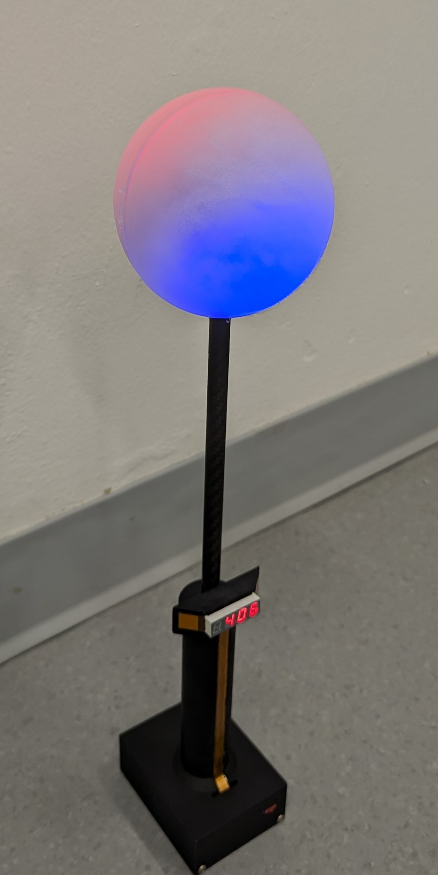
Three visualization modes for the magnetic field vector direction are shown. On left, the nearest-point display. Center, the sphere gradient display. Right, the halo display. The field magnitude in mG (515 to 516) is shown on the 7-segment display.
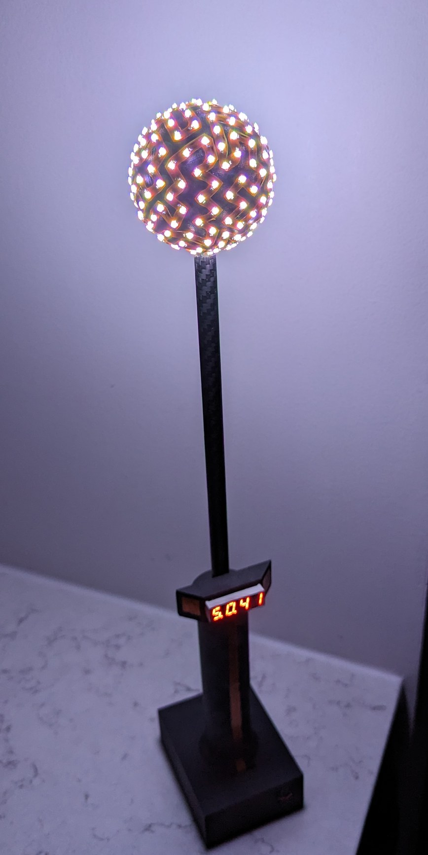
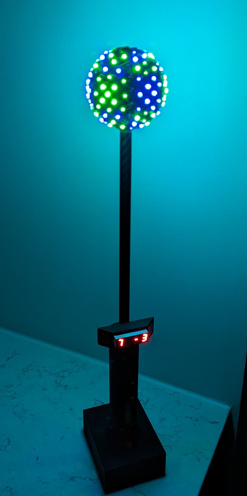
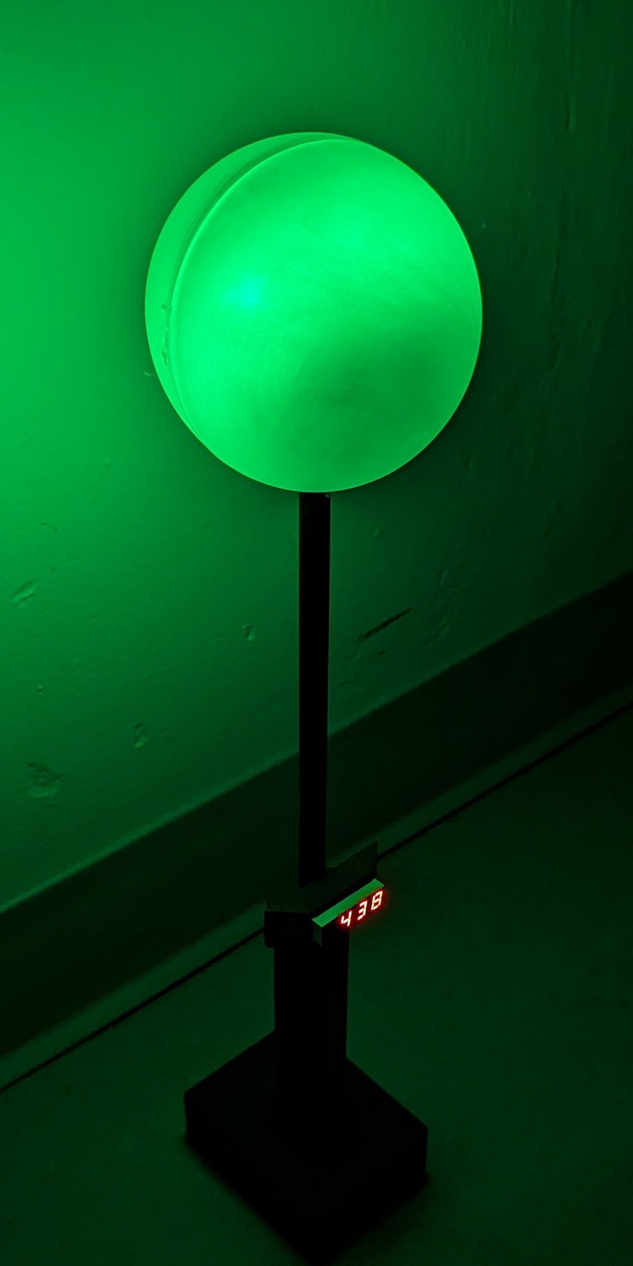
Additional static display modes are implemented. On left, a flashlight mode illuminates the sphere with a uniform color; the 7-segment display shows the current consumption (0.41 A). On right, a spherical harmonics mode displays the magnitude of the real part of a spherical harmonic function Y(l,m); the 7-segment display shows the values of l and m (7, -3).
After some of the build difficulties described above were addressed, the project worked as expected. The magnetic field could be reliably measured to within 1 mG as designed. I found that the magnetic field points mostly downward (at my geographic location) but a small component of it if projected to the ground plane would indeed point mostly north. In large areas away from metallic objects the direction of the magnetic field was effectively constant, while the magnitude could fluctuate by a few mG from a nominal value in the range of 400 mG to 500 mG. In regular residential and office areas, moving the detector by even a few mm would lead to easily observed and repeatable changes in the field magnitude. With the presence of ferrous objects, the magnetic field direction could be influenced, though the effect was more subtle than I imagined. I thought this spherical indicator would reveal complex patterns of field curvature, but the local field is mostly in one direction defined by the earth's magnetic field, and some changes occur within 10 cm of edges of steel objects (edges may concentrate fields due to geometric effects and also due to cold working of the metal increasing its magnetic susceptibility there). The most visually interesting changes in vector direction arise when the field magnitude drops below 100 mG at apparent "inflection points", because at low overall magnitude the angular direction is more sensitive to small perturbations, but these areas are not too common. Steel objects are often seen to be magnetized in the same direction as the earth's magnetic field, with field magnitude increasing to around 700 mG level at the edges or corners that are oriented most favorably if intersected by the field vector, while the edges or corners that are relatively distant from the best-aligned cross section along the magnetic field are somewhat shadowed and may have a surrounding field magnitude that is slightly reduced to around 300 mG level.
It was satisfying to observe a 3D display that would point along a constant line in space as the handle and rest of the device was rotated, and it was a bit of a learning experience for me to learn to distinguish the changes in observation angle (due to the visual effect of moving the sphere relative to my eyes) from the real changes in magnetic field direction (which are subtle when not near metallic objects). Visually, the color and texture of the flex PCB on the sphere generates a distraction from the displayed content, and it is much easier to keep track of indicated direction if the sphere is observed in a dark room (then the flex PCB and sphere surface are not visible). I originally ordered a 3D printed diffuser sphere shell that would cover the indicator sphere, but this part (which was based on some transparent resin that was sanded rough for a translucent surface) did not fit mechanically due to warping in the 3D print. The diffuser is expected to help with the gradient display modes, because visually there is not much difference between a bare LED at low power and a bare LED at high power, of course the latter appears brighter, but this change is minor compared to the one between bare LED at low power and bare LED turned off. A diffuser would help make the brightness change more easily observable because the optical brightness of the nearly point-source bare LED would be spread out over an easily observed area. Despite the fit not being great, I attached the diffuser with a few spots of hot glue to test out its impact on the display's appearance.
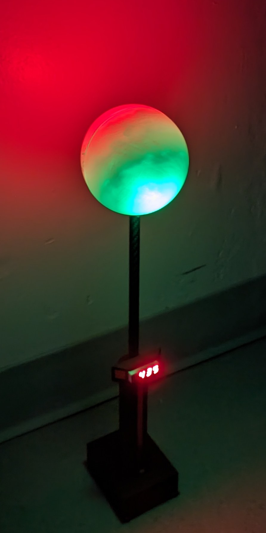
The same three visualization modes as above (in a different location so the indicated magnetic field is different), with a diffuser attached surrounding the LED sphere. The diffuser is a larger spherical shell, with the increase in diameter of similar magnitude as the spacing between LEDs, such that the light cones from nearby LEDs overlap and pixelation is not apparent.
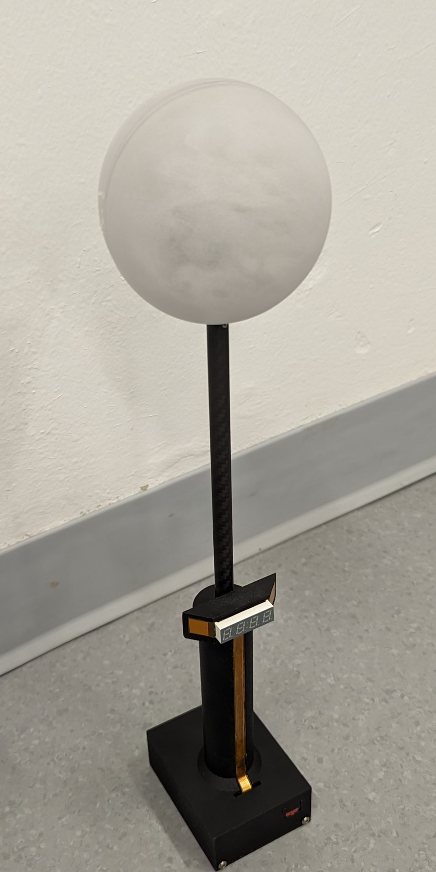
The appearance of the device with diffuser installed when room lights are on. The brightness is reduced compared to the no-diffuser case, but the gradient modes look nicer.
Having a built-in indicator of voltage and current with the INA232 was very convenient. The load switch to the LEDs helped a few times when debugging the LED strips, and it may be used to implement a low-power mode, but otherwise could be skipped. The architecture of the mechanical power switch connected to the LP3873 enable pin, in order to not have the full 3 A flow through the power switch, has worked successfully. The 3 A limit set by the fuse is almost within reach if all LEDs are set to full brightness with a set of fresh batteries, but it was not reached due to the battery resistance (6.4 V at 0 A to 4.57 V at 2.8 A), all the better as the 30 mOhm sense resistor with the INA232's 81 mV input range will only allow reading up to 2.7 A (for the high current test I used an external voltmeter). In the brightest of the operating display modes the total current remains within 0.6 A, and this is found to have no observable effect (at 1 mG resolution) on the magnetic field readings. Of the 0.6 A, about 0.12 A goes to the 7-segment display with Teensy LC (of which the 7-segment display consumes the majority), and 0.48 A goes to the individually addressable LEDs (of which 0.12 A is used regardless of light output). The LEDs appear to be a good size and brightness for this application, and the spherical distribution looks visually uniform with a pleasing symmetry (traces of the underlying octahedron may be seen in the pattern, but they are subtle, and in the display of spherical harmonics, the antipodal symmetry results in a nice appearance). The update rate is visually smooth in terms of both the magnetic sensor and the spherical display calculation (if the device is rotated quickly there is visible lag, but this does not impact normal surveying operation), and the Teensy LC is a great match for this task as the CPU resources and hardware pins are well utilized.
The battery cover for the 3D printed handle could be improved by adding internal ridges which would support the walls of the handle against being pushed inwards (presently such ridges are only placed in corners instead of along the full side lengths, due to uncertainty about the dimensions of the battery holder), and the touch buttons could be made more sensitive by improving the ground plane coupling to the handle (presently one has to grab the handle tightly, in order to place the palm against the ground trace in the 7-segment flex PCB, for the touch buttons to sense a difference in capacitance when touched). While the touch button traces have an ESD protective device on them, I did not add a resistor (100 ohm or so) leading to the Teensy LC pins, so the ESD impulse is not strongly prevented from traveling to the MCU; so far I observed one reset event due to ESD. Another aspect which I did not fully consider was the weight distribution in the device. The batteries are heavy and give a nice weight to the handle (and are confirmed to be far enough away that their magnetic impact at the sensor is below 1 mG), also ensuring the device is not easy to tip over when set upright on a surface, but the tactile experience would be better if the center of mass was raised towards the middle of the handle. With the diffuser glued on top, the center of mass moves up and is then actually a bit too high in the handle, and a less heavy diffuser would be preferred. The diffuser makes the gradient display modes look more visually smooth, as expected, but I prefer to use the device without the diffuser, as the device is then lighter and easier to maneuver, and for me seeing the LEDs directly makes the indicated angle easier to read. The moment of inertia when moving the device seems reasonable, and the sphere is light enough that moving it around to survey a volume is an easy task. I did not rigorously verify that the filter components used in the power supply layout of the main PCB actually helped to reduce electrical noise, but I can confirm that the LED array is updated free of flicker or other indicators of noisy data lines, and that communication over I2C is reliable. The flex PCB connectors did not present electrical issues during any of the initial tests despite slight misalignment and unexpected mechanical loads, and I feel more comfortable using this interconnection method in the future - it is a substantial improvement on soldering individual wires or crimping wires to be used in a header-type connector. The 2-layer flex PCBs themselves have functioned with no issues even after the soldering, cutting, bending, and gluing processes applied in this project, and the LEDs glued on the sphere have remained adhered resistant to gentle impacts. Overall I consider this project a success.
The spherical indicator has worked well since it was built, and carrying it around to different locations has not caused issues with the mechanical assembly. However none of the indicating modes would provide a highly precise indication of the 3D vector, ie the sensor output is more precise than the LEDs are able to show. The mode with single nearest LED would discretize the vector to the resolution of the spherical display, while the gradient modes in principle allow for sub-pixel spacing based on color intensity but the displayed hemisphere regions are extended and do not give a precise visual indication. Therefore an indicating mode was added which lights the three nearest LEDs to the field vector, and the color of the LED that is nearest to the actual vector would be brightest. As the sphere is oriented such that the vector is aligned within a small angular tolerance of a single LED, only that LED would remain lit (the color also changes slightly to indicate the LED is well aligned). It is very easy to tell the difference between one lit LED and a triangle of LEDs, so despite the coarse angular LED spacing, in this mode it is possible to align the sphere to a small fraction of the spacing (to about the angular size of a single LED, or 2 square mm at 30 mm distance). Additionally, I took the opportunity to implement some optimizations - in most indicator modes the antipodal symmetry is applied to halve the calculation time, and in the nearest-LED mode the squared distance is used in comparisons to avoid an unnecessary looped sqrt() call. A free cycles counter is added to confirm that none of the indicating modes cause a delay in the nominal poll rate of the magnetic sensor, set by a constant delay of mmc_delayms=11; the slowest mode is the three-LED indicator but there are still 194 free loop cycles available (with no indicator active, this value is 762). The new firmware files may be downloaded here.