As a long time fan of rhythm games like Dance Dance Revolution (DDR) and Pump It Up (PIU), I wanted to have my own dance pad / stage which would be used as a controller for games like StepMania. Previously I ordered the StepManiaX Gen 4 stage, which worked well enough but some improvements could be made. Beyond the electrostatic discharge issue which would cause the stage to periodically reset if used in the dry winter air, the mechanical design of the arrow pads and sensors was not to my standards. This is because the pads were quite loose and could move laterally, and there was no clear delineation of a mechanical parameter that would control the sensitivity of the Force Sensing Resistors (FSR) underneath the pads. Instead this sensitivity was reliant on the combination of mechanical deformation, FSR response, and electrical calibration, with the first two physical parameters being impossible to adjust incrementally. A layer of foam under the plastic surface would be compressed to provide the spring action, however the foam would be subject to tearing and permanent deformation due to a small contact area and lateral motion of the pad. The loose attachment of the top surface was in turn necessary because if it were tightened down the variety of mechanical influences on sensitivity could not then be countered by the calibration in software. Such issues can be solved with a different pad and sensor design, which is what I set out to do in this project.
The mechanical engineering problem of a good pad design is rather tricky. This is because in an ideal case the pad should last a long time, handle high forces such as jumps and strong hits (including lateral forces), and also respond to even light touches for fast technical play. Further, the light or heavy touches on the pad may come from any edge or corner and should be processed in an equal manner. For my design, the particular aspects I was looking for were:
Towards these goals, I came up with three different approaches:
All of these derive from the traditional solid pad design which has force sensors attached at the pad corners or edges measuring the force by deflection or displacement of some electrically conductive materials. Hence they share the same issue: they require displacement and the associated mechanical challenges. If the sensors are made robust enough to handle the force of jumps, then it is difficult to measure light touches, and vice versa (there are sensor designs that achieve this, such as based on a deflection of a tubular structure). And there will necessarily be moving parts, even if ideally the displacement is elastic in nature. Can we eliminate displacement and thus have a solid pad? This will remove the downward motion of the pad and the associated tactile feedback, but really the displacement is about 1 mm anyway, and that is not felt during gameplay. Then we may as well advance into the future and jump on the bandwagon of:
Just like touch screens on mobile devices, which have no moving parts and can detect light presses, we can make a capacitive sensing pad which will be mechanically robust and responsive. All sensitivity adjustments can be done in software, and there are no mechanical adjustments or wearing parts. The question then becomes how to design what is basically a large capacitive touch sensor. A capacitor is formed of two charged surfaces, of which the pads make one surface, but then where is the second? It is possible to have the player as the second surface, by connecting the player to electrical ground, such as with a wrist strap used for handling ESD sensitive devices, and this would make for a very high touch sensitivity but playing while tethered to a wire is not very fun. (Note that if you exclusively play while holding the bar, the bar could be grounded and this approach used; initial testing shows that this will even work while wearing shoes.) Then, if the player is ungrounded, capacitive sensing would rely on the player's body enhancing the connectivity between the pads and some other grounded surface. The most obvious place for the other grounded surface is next to the sensing surface on the pads: the foot placed on the pad would then complete a connection between a sensing conductor and an adjacent grounded conductor, increasing the measured capacitance.
With this principle, a sort of interdigitated electrode surface was envisioned. I made a cheap and quick prototype from a piece of foam board and aluminum foil glued on with a spray adhesive then cut into the appropriate shape. Within an approximately 12x12 inch area, there are two conductive surfaces nested inside each other, and the capacitance is measured between the two using a digital multimeter. With the salty water content of a player's foot (ungrounded) replacing the air above the sensor, the measured capacitance is expected to increase. Trials with the quick prototype confirm this: the capacitance increases from 70 pF to 110 pF when touching the foil surface with the tip of the foot (wearing socks). With the whole foot placed on the pad, the capacitance can exceed 150 pF. The capacitance value is robust and stable over time. The capacitance has a rapid fall-off with foot distance from the pad, so it should be easy to set up a software threshold that will not respond to foot "hovers" but only to presses. However, this design does not seem realistically suited to use with shoes. This is because with the increased vertical separation between the foot and the pad due to the shoe, the capacitive threshold needs to be set very near the base (no-contact) capacitance, which in turn makes the pad more susceptible to spurious and "hover" activation. The same problem exists with gloves and capacitive touch screens. As this will be a home use pad where I only play in socks, there is no concern in using this design, but for commercial installations where players are expected to wear shoes, it will be necessary to go back to the drawing board and pick one of the displacement based approaches (this does not rule out capacitive sensing though - one could well sense displacement via the capacitance between two conductive surfaces of which one is displaced).
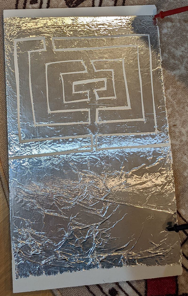
Photo of the quick prototype of interdigitated capacitive touch sensor pad. The width is 12 inches and sensitive area height is 12 inches. The red and black probes attach to a multimeter that measures capacitance between the two conductive foil segments.
With the general concept proven to work, I wanted to make the final design based on a more rigorous evaluation of the influence of sensor geometry on the capacitive response. The parameters of concern are conductor width and separation between conductors. In the prototype above I free-handedly picked about a 1-2 inch width and a 0.2-0.4 inch separation which worked well enough, but could it be optimized? From intuition, it seems that making the conductors too narrow will reduce the coupling through the foot which is not advantageous, and putting them too close together will increase the no-contact capacitance, which is also not great. So having a width of about 1 inch (about half the width of the foot) and spacing of about 0.25 inches (about the thickness of socks and other pad structures above the conductors) seems reasonable, which is confirmed by the electrostatic simulations. I simulated the pad using the electrostatics module of FEMM 4.2 (and planar problem type), by measuring the capacitance between two conductor lines at different sizes and spacings in the presence of air or water at a certain height above the conductor. In this way I have a measure of the no-contact and contact capacitance, to check the sensitivity of a particular pad design. This is automated using LUA scripts to vary the air gap and conductor width.
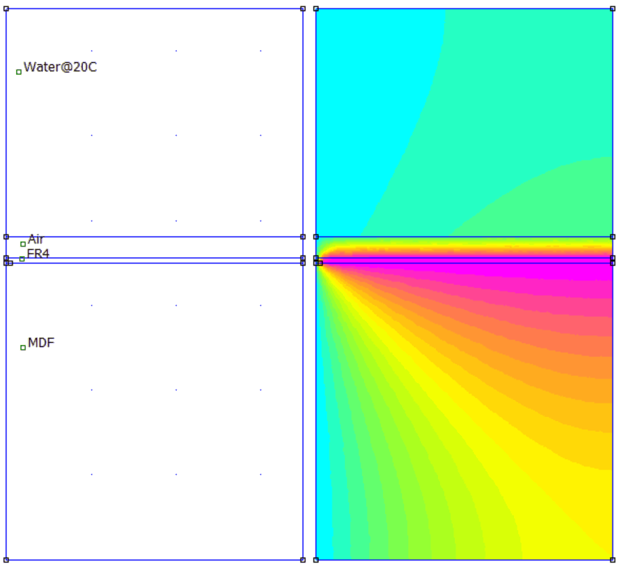
A planar electrostatics simulation using FEMM 4.2. The left edge is defined as 0 V to satisfy the symmetry condition, and the right side of the central horizontal line is defined as a 1 V conductor. The simulation calculates the resulting charge from which capacitance may be determined. The colors in the figure on the right represent different voltages from 1 V along the right horizontal to 0 V along the left vertical. A thick layer of MDF is below the conductor, and above is a thin FR4 layer representing the PCB and an air gap to a thick water layer representing touch contact. The dimensions are varied to check how the capacitance responds to touch proximity with different sensor geometries.
The general trends are:
In fact the simulations were already conveying a message I did not appreciate until later: the base capacitance comes from the interaction of the conductive surfaces beyond the "intended" path. As the base capacitance is approximately half of the touch capacitance, the effect is substantial, and in itself can be used as a sensing mechanism. We will return to this topic in the second iteration of the build.
Once again I turn to the venerable Teensy LC as the microprocessor for this project. The Kinetis L series ARM Cortex MCU (MKL26Z64VFT4) used on the Teensy LC has an integrated hardware capacitance touch sensing input (TSI) module. This includes an internal current source and voltage comparators to charge and discharge an external and internal capacitor, with a counter to count the relative number of charge and discharge cycles. I mentioned this possibility in the keyboard style touchpad project where it was left unexplored because I wasn't sure about the timing and sensitivity of the TSI module, in fact it seemed too easy and too good to be true: just connect some conductive surfaces to the pins of the Teensy LC, write a few lines of code, and you have a capacitive touch controller. Here I confirm that it really is that easy and that good; if you want to put in the minimum effort then just run some wires connecting some pieces of foil to the Teensy LC pins and you're done with the electronics. Various parameters can be tuned in software to achieve scan times under 0.1 millisecond per button, and the capacitance results are both accurate and robust.
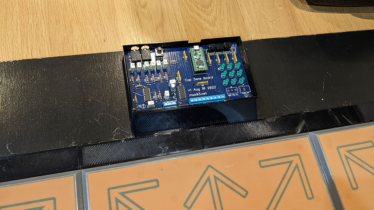
I wanted to put in a bit more effort to get a neater finished product, and made a circuit board to interface the Teensy LC and the capacitive touch sensors. The primary reason for this was to add in some external electrostatic protection, because with the likely triboelectric charging of the pads during gameplay, it can be expected that discharges will occur. The MCU does have internal ESD protection, but I prefer to not rely on that as directly interfacing with the pads seems too severe. Each of the lines running to the pads is paralleled to an ESD protection IC (SP720APP TVS Diode Array, labeled R4 on schematic), and passes to the Teensy through a 100 ohm resistor so that if a transient occurs it will be preferentially absorbed by the IC. I'm not sure whether the power bypass topology I used for the IC was a good or a terrible idea, so it would probably be good to check with an electrical engineer before copying this approach. The protection IC will present a low impedance during an ESD event, and if it is passed straight into the power rails this risks resetting or damaging the MCU, so perhaps defeating the point. Instead the static protection IC has a 220 uF low-ESR electrolytic capacitor along with a 1 uF film capacitor (fast and low-ESR) connected between ground and 3.3 V lines. Then a 10 kOhm resistor links that to the 3.3 V supply on the Teensy. Hopefully the ESD event is then absorbed into the capacitors and slowly discharged into the power supply. The ground is connected without a resistor so it can equalize rapidly. Just in case, a 4.6 V Zener diode is in parallel with the capacitors, to handle any prolonged discharges, but it is doubtful whether this is needed or even helpful (after all the IC latches on the voltage exceeding the supply voltage, so if we allow the supply voltage to increase, will it continue to run as expected?).
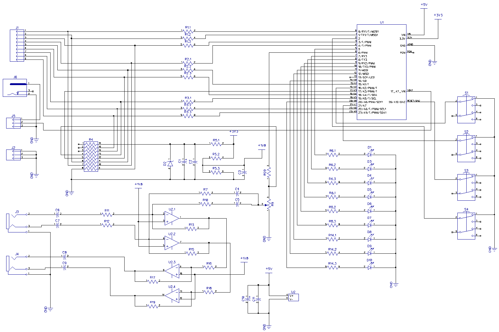
Schematic of the Teensy LC interface board. Designed using DipTrace. This may also be downloaded as PDF here. A list of component part numbers and links may be downloaded here.
Beyond the primary feature of ESD protection, the circuit board was designed to offer the following:
The push buttons are fairly self-explanatory. I use 4 latching DPDT buttons, although only one P and one T is used on each (the DPDT ones were cheaper than the alternatives). Pull-up resistors are built in to the MCU, so there are no more components to add here. The indicator lights are 9 LEDs passing through 470 ohm resistors. As with the ESD IC, the resistors here are in a combined package which simplifies assembly and makes for a cleaner looking board. Is it wrong to use 13 pins of a very capable MCU just to read 4 buttons and drive 9 LEDs? What is wrong anyways? If right cannot exist without wrong, then do I have a moral duty to do wrong? In any case, it is simple and fast. For any additional lighting I route the 5 V amplified pin 17 output of the Teensy LC to a separate terminal block so one can use individually addressable LEDs, but this will not be done presently.
The audio mixer and amplifier section is intended to take a stereo audio signal in a 3.5 mm jack, add to it a feedback tone at the moment of touch button press, and output the summed audio in another 3.5 mm jack. This is just a standard inverting summing amplifier followed by another inverting amplifier, for each stereo channel, done with a quad op-amp IC. A potentiometer allows manual adjustment of the feedback tone volume, while the input audio is passed through at unity gain. I think getting auditory feedback with minimal lag is a useful tool for improving performance in rhythm games, so the concept is worthwhile, but I designed the amplifier section in a rush. There are plenty of problems with this section which will be discussed later.
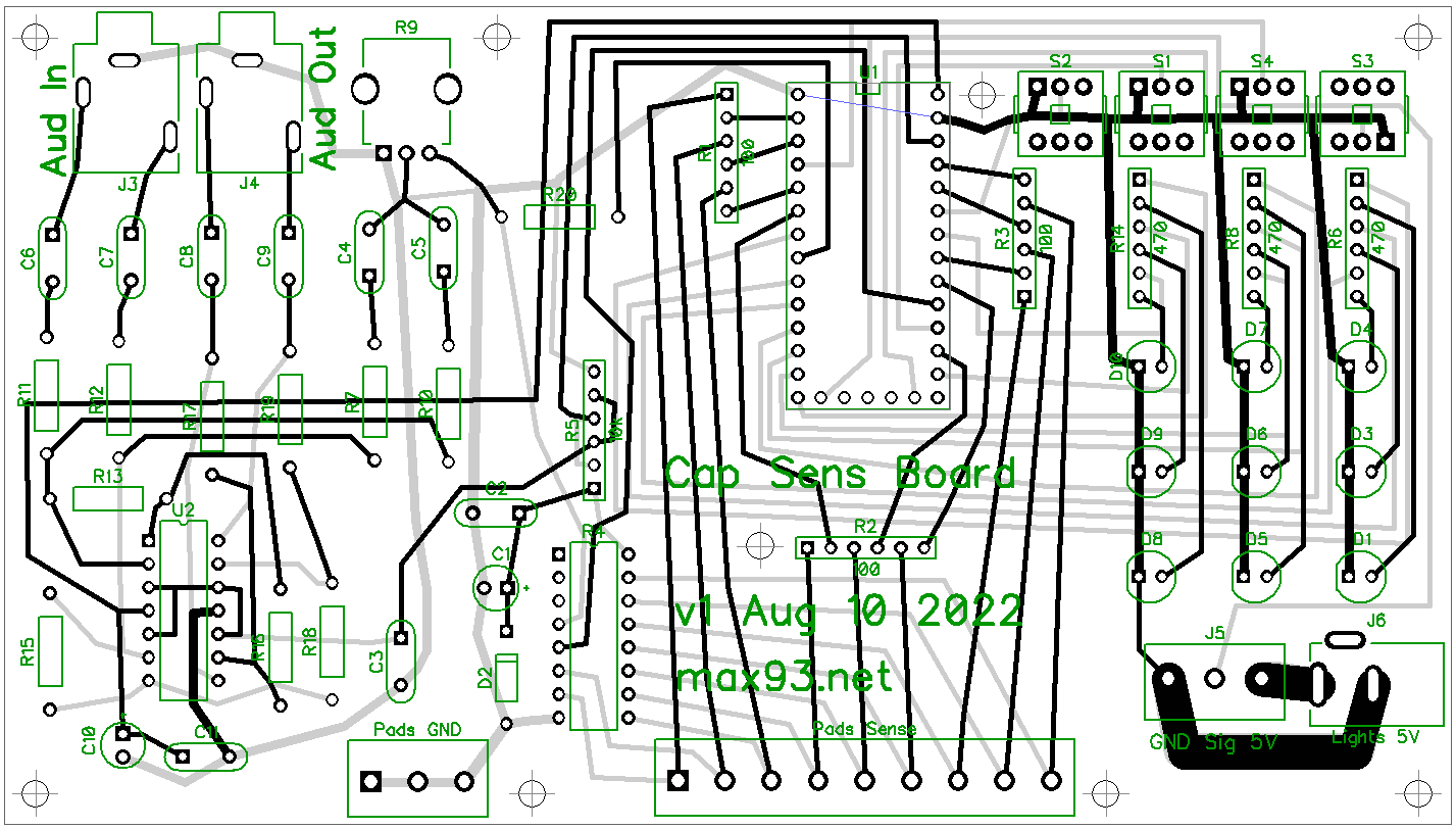
Layout of the Teensy LC interface board. Designed using DipTrace. This may also be downloaded as the source DipTrace (.dip) file here.
I routed the board so it uses wide and generously spaced traces, and also uses no vias (connections between the top and bottom layer are all done through the holes for components). This makes the board easy to fabricate on even a questionable quality CNC mill, and also means that layers can be connected by soldering on both sides of certain component legs so there is no need to have plated holes. I also allowed for the possibility to not install components on the board which are not needed, so a very minimal build could just include the static protection and Teensy LC and nothing else. For instance the bottom row of Teensy pins is used for switch 4 and external LED control, and I do not use these features here so those pins and components will not be connected. All components are through-hole because I've reached the limit of my patience on soldering surface mount components with an iron. The spacing of the capacitive sense traces is important because, of course, they sense capacitance, so on the board they are far apart from each other and from any ground traces. I made no effort to hide the manual routing so there are few neat vertical and horizontal lines on the board, but it functions just as well. Also the priority was on ease of connection of pins to hardware on the board, rather than matching pin numbers to specific functions, so for example the order of touch pads 1-9 and indicator LEDs 1-9 in terms of Teensy pin numbers is not an ordered sequence but a combinatorial jumble. Perhaps this is an obvious optimization, because setting up the pins in software to match the hardware (after routing per convenience) takes just a line of code, while routing the board to match pre-determined pin numbers can be very annoying, yet I want to highlight the possibility for anyone who may not have used it before - doing this necessitates a change in the workflow because the typical approach is to assign pins in the schematic and keep them fixed during routing, whereas here I started with the routing as a means to guide pin assignment.
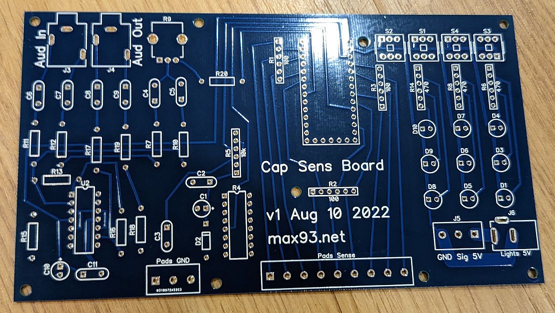
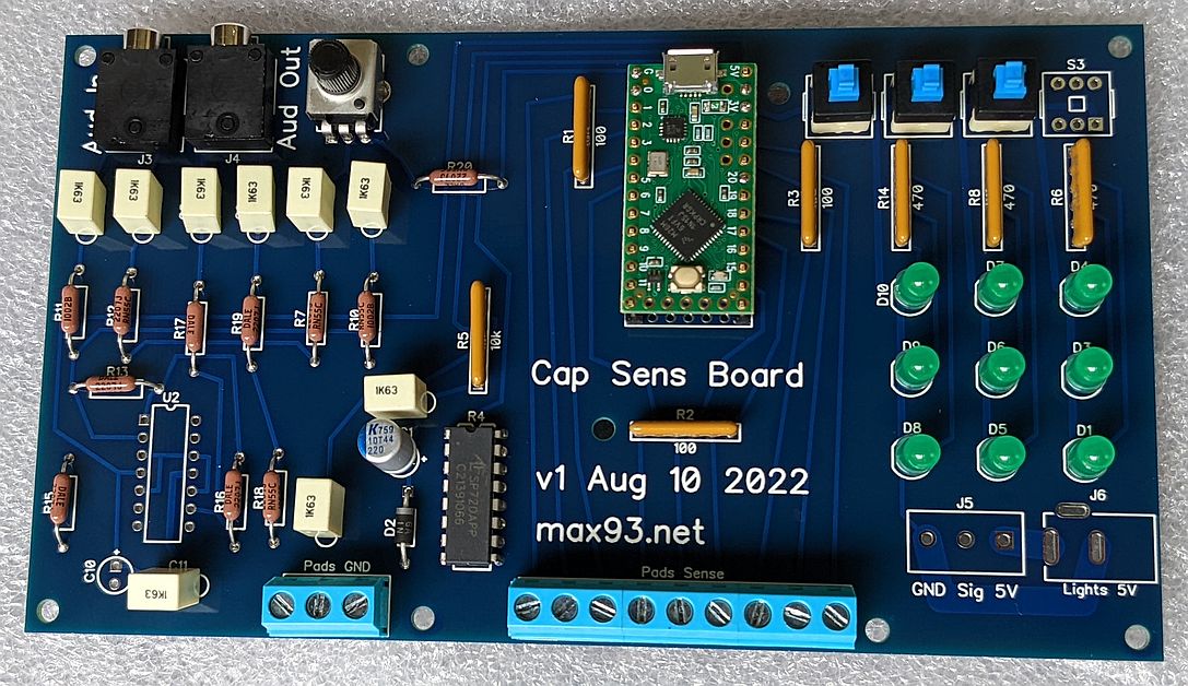
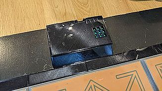
Photo of the Teensy interface PCB, on left as received from manufacturer (pcbway.com), on right after soldering the components. I soldered this using the new style miniature low-power (12 W) soldering iron while sitting in the back of a car, and it worked surprisingly well.
Based on the electrostatic simulation results above, the capacitive sensor board was designed as a 1-layer grid of approximately 2 inch wide squares which alternate in being connected to the sense pin or ground. Wires may be soldered to the surface at the corners, with the ground connection passed along the sides to remove the need for extra ground wires.
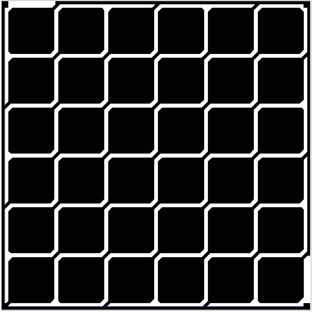
Layout of the capacitive sensing board. Squares are connected along diagonals, alternately to sense pin or to ground. Designed using DipTrace. This may also be downloaded as the source DipTrace (.dip) file here.
The Teensy LC has a hardware module to measure capacitance on some of its pins. With the Teensyduino installation there is an included function touchRead(pin), however to have more control over the measurement process (such as the internal and external charge currents and count prescaler), the program here accesses the associated registers directly. It is thus specific to the Teensy LC. The code file CapTouchTest.ino shows a basic use of the TSI registers. There is also a way to use the TSI module for noise sensing (which is similar to what I did earlier with the keyboard style touchpad, except there I used external op-amps) but the documentation on this whole topic is very obscure. The final code file Touchpad9.ino has filtering on the button press and release (time and hysteresis), configurations for high and low sensitivity, and live calibration of the key capacitance thresholds during gameplay (which isn't really necessary because the base capacitance is stable, but helps in case of noisy or spurious readings). If compiled with the Serial + Keyboard + Mouse + Joystick option, it is possible to connect to the Teensy LC as a serial device and modify settings. For example, sending :S1 will enter the Status Update Mode, where every second the capacitance measurements will be sent to the PC, and the onboard LED pin will toggle after every loop completion (by this means it is possible to verify the update rate of the pad). The full list of commands may be gleaned from the comments in the processCommand() function.
The live calibration and filtering features make this code quite robust. I was able to get a usable controller with a wide variety of capacitive sensor configurations as "plug and play". Note that presently the live calibration only uses the minimum measured capacitance to calculate a new threshold, but it should be easy enough to use the maximum as well, which would make the controller even more versatile. (I have not done so because it will not be useful for my application and would introduce a possible mis-calibration vector.) Switch 1 activates '+' mode which is used for DDR, while switch 2 activates 'x' mode used for PIU, and switch 1+2 activates all 9 buttons. Switch 3 sets either high or low sensitivity threshold presets. Switch 4 sets player 1 or 2 button mappings, which really isn't that useful and is more of a placeholder in case I later come up with some clever feature. (I don't include the physical pushbutton for switch 4 either in this build, although the space is there on the PCB.)
Scan times (polling all active buttons) of slightly over 1 ms are obtained in the + and x modes and slightly over 2 ms in the full mode. This time may be decreased further by decreasing the hardware prescaler and scan number counter in the TSI configuration, but there isn't really a need to and I suspect using too short of a time will increase susceptibility to noise. There is interleaving in the code so that some useful work is done during the hardware scan period, however the time gain from doing so is minimal (about 1 percent) because there is not that much work to do - most of the polling time is spent waiting for the hardware scan to finish. In principle this is a case where DMA would come in handy, however I could not figure out any way to get the DMA to work with the TSI module (maybe it only does so when exiting low power mode?), and even if I did get DMA working, the only thing that would achieve is being able to put the CPU in low power mode because it doesn't need to do anything in the meantime. So I will consider the ~1 kHz update rate a success and not complicate things further.
For the capacitive sensing pads, I decided to buy them as large one-sided PCBs from pcbway.com to save on manufacturing work (because now I don't have access to any workshop machines or tools). In designing the PCB, I used a diagonally connected square pattern instead of the C-shape interdigitated pattern of the foil prototype. The square pattern is easier to draw, but has the limitation that half of the squares along the edges are grounded and are not sensitive to touch, so if the foot comes in from the edge over the grounded squares there is no response. In the C-shape pattern most of the outer perimeter of the pad is the sensing surface, so this does not occur, which is why I used that shape to begin with. I hoped that somehow this issue with the square pattern would not be a major effect, but it does occasionally cause skipping a desired keypress during gameplay, and this will be remedied in the next iteration.
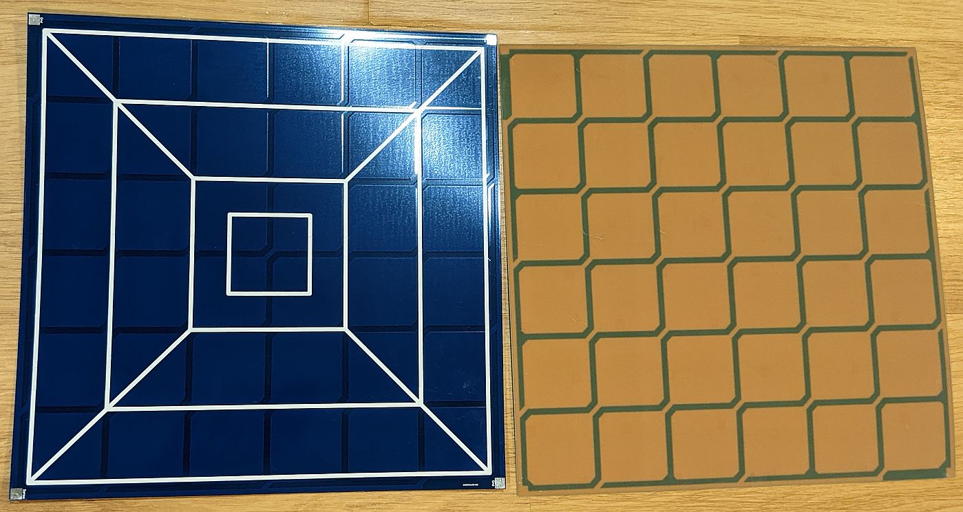
The top and bottom surfaces of the capacitive sensor board. Each board is a bit under 12x12 inches. Any two adjacent squares (along the vertical and horizontal) connect to two different electrodes for the capacitance measurement.
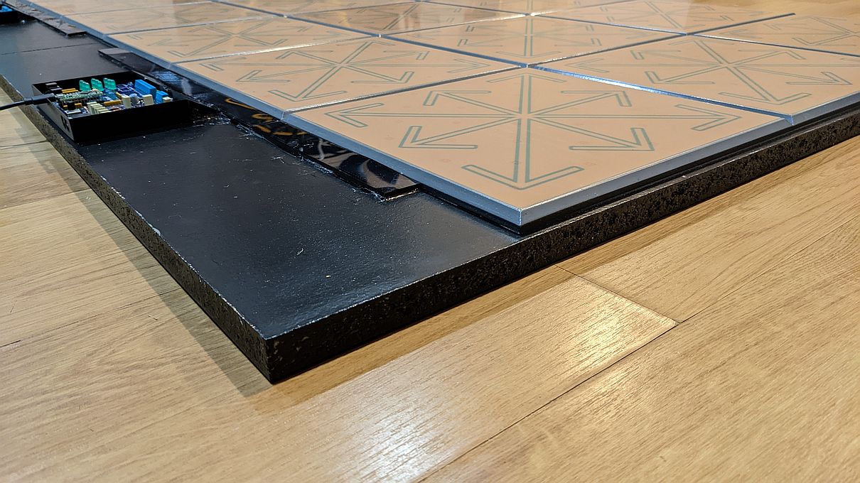
The main structure is made out of a 3/4 inch thick particle board, which I bought at Home Depot and they cut it to size for free. Particle board is cheap (vs plastics and metals), has low impact on measured capacitance (vs plastics and metals), and is uniform in dimensional properties (vs plywood or solid wood boards). The main advantage of having a thick base like this is its weight so it is less likely to move around during gameplay, however the capacitive sensor design really doesn't require much vertical space so the build could be ultra-thin. To create a flat top surface, with the wires for the capacitive sensing boards soldered on, the boards are glued (using an aerosol spray glue) to a piece of hardboard that is cut to the same outer dimensions. The hardboard piece raises the PCB off from the base particle board by 1/8 inch, so the wires to the PCB are below the new top surface. The ground connection is the same on all pads so a trace on the PCB is used to connect them instead of a separate wire running alongside (to reduce the non-contact capacitance).
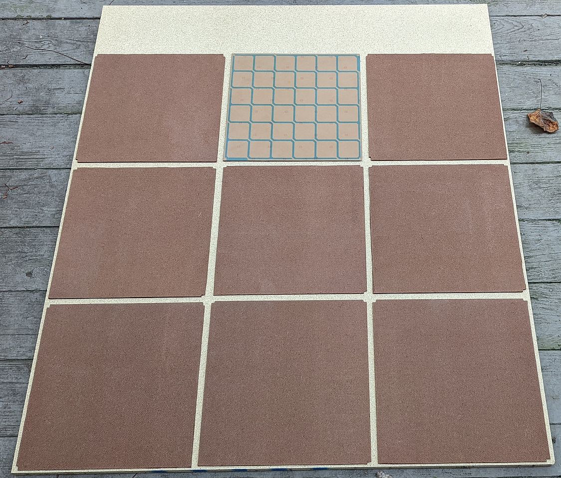
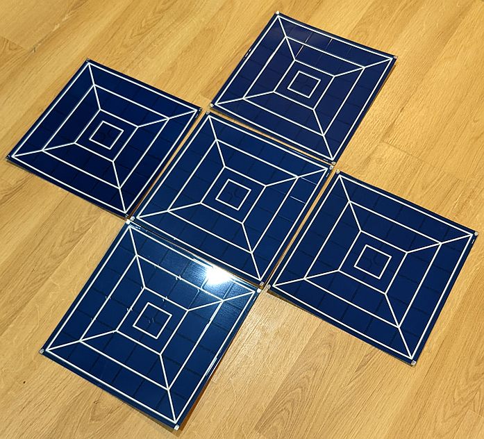
Laying out and gluing the capacitive sensor PCBs to the particle board base. On right, the finished 9-key pad with interface board connected.
This worked well enough, however a few issues and findings surfaced that caused me to go back to the drawing board:
In particular the last issue, of the grounded squares compromising the useful sensor area, was troubling. An "obvious" fix might be to use an array of switches to swap the ground and sense connections during each scan, so that the entire surface area is sensitive. However this would require a lengthy and probably expensive redesign of the controller board. To see how I might otherwise improve the sensor PCB, I experimented with disconnecting the grounded sections of the interdigitated squares and connecting them to the sense wires. The results were surprising: I could completely remove the ground connection to a lot of the sensor boards without a noticeable impact on their sensitivity, and I could even improve their sensitivity by connecting the previously grounded squares in parallel with the sense squares. This is counter to the typical intuition of how this capacitive sensor works. More surprisingly, if I removed the ground connection to all of the sensor boards, then the non-contact readings dropped to a very low value and touch sensitivity was effectively zero (regardless of whether the computer to which the board was connected via USB was connected to the power outlet ground or not). Reliable measurements could be resumed by connecting to the ground pin a large piece of foil (over 2 square feet) held in close contact with the floor. (I drew the same conclusion in the keyboard-sized touchpad project: noise immunity requires the physical presence of a large grounded conductor.) I thought that maybe there is a radio-frequency resonant effect where the body acts as an antenna drawing excess current when in close contact with a sense conductor, and a human height is about a 1/8 wavelength for a 19 MHz signal; however varying the sense signal frequency (by changing the charging current) by an order of magnitude did not change the sensitivity, so this effect is likely minor. (Still such radio-frequency resonance sensing may be an interesting idea to try because it opens some unique possibilities.) So in all, the best explanation I could come up with is illustrated below:
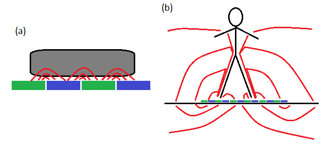
In (a), a conventional interpretation of the interdigitated capacitive sensor: the blue and green rectangles are the differently charged conductor surfaces, and the red lines are electric field lines passing through an object near the surfaces. The presence of the object near the differently charged surfaces increases the measured capacitance. In (b), we look at the bigger picture for a large capacitive sensor as built here: then we must consider the field lines passing through all grounded surfaces including the floor and walls around the player, which will all contribute to measured capacitance.
Namely, it is not adequate to just consider the field lines on the top surface of the sensor; the lines passing not just on the "inside" but also on the "outside" of the capacitor must be included - these go through the particle board base, through the floor, through the walls around the player, through the ceiling, through the air, and eventually find their way back to the player and through the player's conductive body towards the foot touching the pad sensor. Even though these "around-the-player" paths are long and high-resistance, they are more numerous than the few paths between the sensing conductors in the air above the sensor, so their contribution cannot be overlooked. When some of the ground connectors on the pads are disconnected, the charge loop may be completed through any remaining grounded conductors (in physical contact with a large surface area of the literal ground or floor), but when all of the grounded surfaces are disconnected, the charge loop is no longer effectively completed so sensitivity drops to zero. My testing with the large capacitive sensor pad suggests that "around the player" paths contribute most of the sensitivity ((b) in the image), while "within the foot" paths are a minor contribution ((a) in the image). Hence there is no need to have a ground plane co-located on the sensor PCB, but there is a need to have a ground plane.
The above findings set the bearing towards a new design. The sensor board does not need to have interdigitated grounded (non-sensitive) regions, and instead may be as simple as a solid conductor square. The board itself should be smaller, and the spacing between the pads should be smaller as well. Wires should be protected and neatly hidden under the sensor structure. The approach here will be to use an MDF tile milled with length-wise slots on the underside and edge chamfers, such that the sensor board can be glued on top and the connector wires inserted within the slots. At first I was tempted to call for a milled top surface pocket into which the PCB would fit resulting in a flat surface, however this would require a painful process of matching at least 3 parameters (length, width, height) between the PCB and the milled MDF - easy enough to do in CAD but bound to lead to trouble when assembling the final product. Instead I would glue the PCB on top of the MDF, and then fill in the gaps at the edges with a polyurethane compound; the PCB corners are rounded so there is not a sharp initiating point for adhesive failure. If I had the ability, I would vacuum form a thermoplastic sheet to cover the top of the tile, but for the time being, applying a compound by hand and letting it cure is good enough. The tiles are reduced to 11.25x11.25 inches, still not the arcade 11x11, but my reasoning for the larger tiles is that when placing two stages side by side for doubles play the "dead space" in between the stages is reduced. (Did I mention I am making two of these?) Also with a 0.25 inch chamfer applied on the top, the size of the sensor board is 10.75x10.75 inches, which is a bit under the arcade square. I think this is a decent compromise and the difference is not noticeable during gameplay.
Given that the ground plane does not have to be on the sensor board, it is tempting to just use a solid square conductor as the sensor element. I did not do so for two reasons: first this would not look very interesting visually, and second the ground plane still has to go somewhere. Short of making a metal foil "sandwich" under the wood base of the stage, the easiest and most convenient place to put the ground plane is co-located with the sensing plane. Therefore I kept the general idea of having a grounded conductor on each sensor board, but I changed the shape of this conductor. Its area was reduced to 1/9 of the remaining area, meaning that with 9 sensors the amount of copper on a given sense wire (since they are scanned one at a time) would be approximately equal to that on the ground wires (which are always connected). An arrow motif was chosen to match the rhythm game style, and to save on manufacturing costs I just put all the arrow directions on there so an identical layout could be used on all sensors. All the outside edges were left as solid sensing conductor, so that the edge non-sensing issue of the interdigitated square design would be remedied.

Updated layout of the capacitive sensing board. The arrows are connected to ground, while everything around them is the sensing surface. Designed using DipTrace. This may also be downloaded as the source DipTrace (.dip) file here.

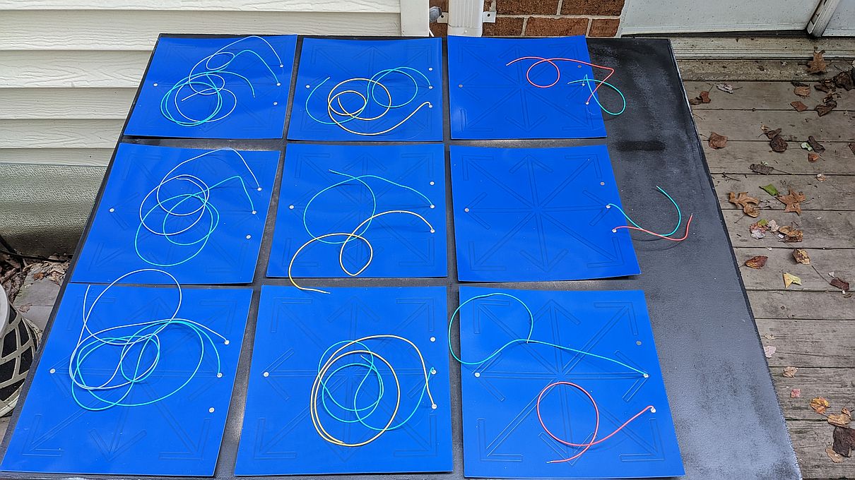
Photo showing the manufactured one-layer sensor PCBs. Wires (24 AWG stranded) are soldered vertically onto 0.25 inch diameter circles on the PCB to later connect the conductor surface to the controller board. Different wire colors are used for different rows to aid identification later when the wires are underneath the board.
While at this early stage of the build, I wanted to incorporate some changes to make the final product look more interesting, namely painting and coating the wood (particle board and MDF) base structures so they look sleek and shiny. The photo below shows the starting point and tools.
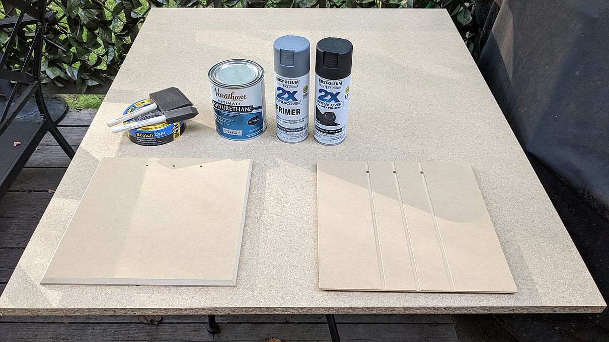
On top of the as-purchased particle board, there are: Varathane polyurethane water-based sealer can, Rust-Oleum gray primer and flat black spray paints, a roll of blue masking tape, and 1-inch and 3-inch foam brushes (I used 3 of each). Below these things in the photo are two milled MDF tiles as-received, the one on the right flipped upside-down so the grooves for the wires are visible.
I began by spray-painting the particle board black on one side and all edges. Then the MDF tiles were spray-coated with primer (is that considered painting?) along the edges which would remain visible after the PCB is glued on top. I did not spray paint the top surface of the base board nor the top surface of the tiles, both to save paint and to leave a more grippy wood texture for the glue that will be applied later.
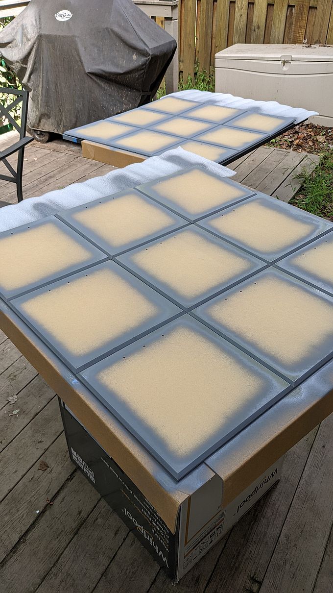
Spray painting the visible edges of MDF tiles outdoors.
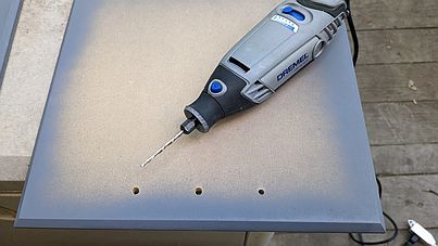
Holes drilled in each tile allow the wires from the sensor board to pass into grooves milled underneath the tile. To finish the edges of the hole while maintaining a flat top surface a downward-cutting dremel bit was used: this has a counter-clockwise flute direction and the flute is sharpened on the bottom, so that the cut material is pushed downwards and a clean top edge is left.
Once the spray paint is dry, it is time to glue the sensor PCBs. For this purpose a can of 3M 77 spray adhesive is used. In the background, I use the 3 inch foam brush to apply coatings of polyurethane to the back of the particle board base, so that they dry while I do other work. I set up somewhat of an assembly line, with an MDF tile coming in, receiving a coat of spray adhesive, then the adhesive dries for a few seconds while I prepare the PCB, then I align the PCB and press it down. The wire lengths and locations are different on each pad so I keep track of the order in which they are glued.
Laying out the sensor PCBs prior to gluing.

After gluing, a heavy box is used to compress all the tiles underneath. From this angle it can be seen how the wires fit in the grooves under the tiles. Extra MDF tiles are placed on top and bottom of the stack to spread the weight more evenly.
With the PCBs glued to the tiles, it is tempting to do a quick test. Here the tiles are laid out on the floor without any other attachments. The capacitive sensing works but is noisy, because there is no solid ground connection yet. The office chair legs at the top of the photo may give a sense of scale.
With the sensor PCBs glued to the MDF tiles, I have to start on what is probably the most annoying phase of the project (in fact so annoying I didn't even take photos). It is not difficult and in real terms doesn't take that long, but with every slow and careful brush stroke (to keep the PCB clean) a doubt arises in my mind, "is this really the best you could come up with?". Well, given all the constraints, I couldn't think of a better solution. The phase is: applying polyurethane to the edges of the sensor PCBs, in order to fill in the 90-degree triangular gap between the MDF tile chamfer and the PCB top surface. This really makes a difference, not only because it prevents lateral foot motion from tending to pull upwards on the PCB edge and causing delamination, but also because it turns the MDF chamfer into a smoother and harder surface. I applied a total of six coatings to adequately fill the gap and leave the chamfer with a hard and somewhat slippery surface. The design presented here would not be usable without a coating like this, as the bare MDF has too much friction and easily tears away in little bits. Still, a thermoformed plastic sheet would look a lot neater. I think I have intuitive concerns about the polyurethane delaminating, but my engineering knowledge counters that with the chamfer geometry and loading this should not be an issue - time will tell. After a few days for the polyurethane to fully harden, the tiles are ready to be attached to the base.

Gluing the sensor tiles to the base. Here the two lower rows are completed while the upper row is still missing. The wires for the lower rows can be seen extending vertically, and they will later be covered by the upper row tiles. These tiles can be seen (flipped upside down) towards the top of the photo.
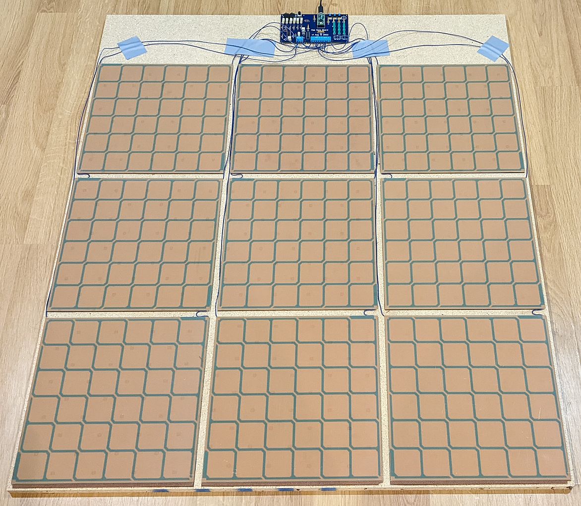
The tiles are glued to the base using the same 3M 77 spray adhesive. Wires are fit into the grooves underneath the tiles, and hot glued in place to prevent movement from the expected vibration during use. After another day of compressing the glued joints using a few chairs and suitcases, the stage is almost completed. The controller may be wired up now for testing and performance validation.
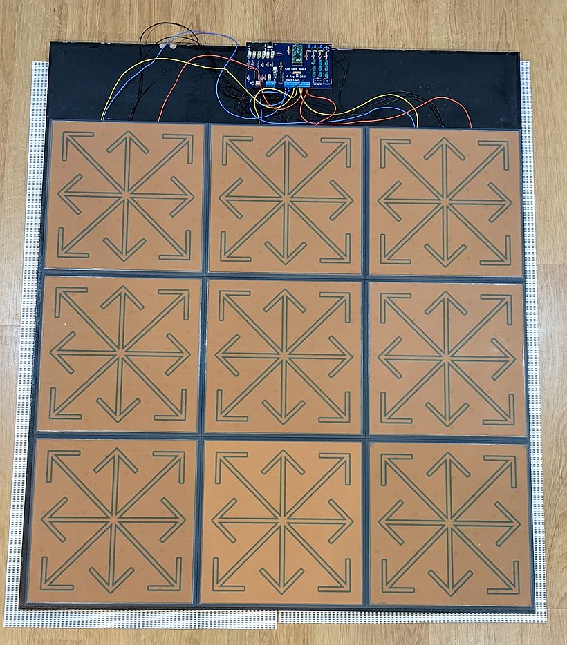
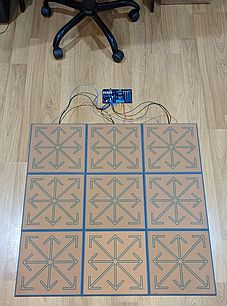
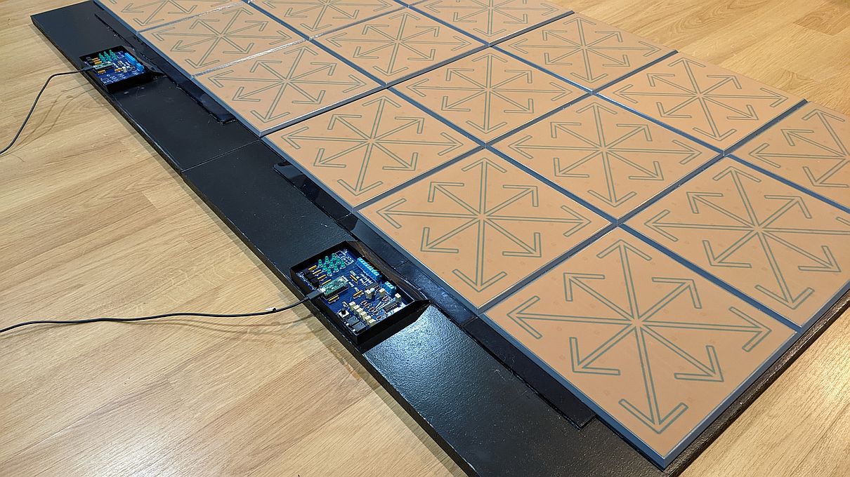
A top view of the stage after final tile gluing. The controller board is connected and the stage is placed on top of a white rubber-like shelf liner for increased stickiness on the floor to avoid sideways sliding during gameplay.
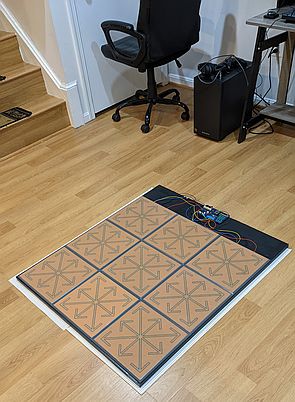
A view of one stage from the side. Furniture and other objects give a sense of scale. The base is 34x40 inches.
Having confirmed that the capacitive sensing works as intended, it is time to tie up loose ends. The exposed top surface of the particle board receives a few coatings of polyurethane, wire covers are 3D printed to create a neater look, and wires are trimmed to fit within the covers. I also 3D printed a cover for the controller board, but I think the stage ends up looking more interesting with that cover left off. Then the project is complete!
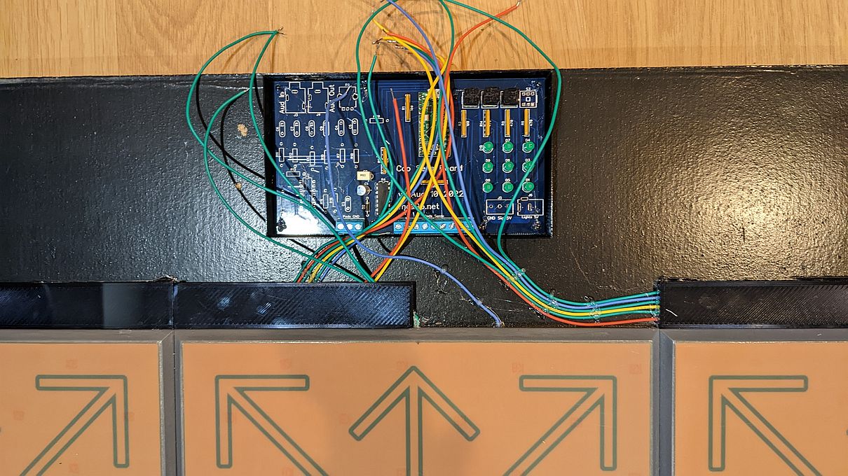
Taming the tangle of wires: the wires coming from the top of the tiles are hot-glued onto the base board within an inch of the tile edge, and a 3D printed cover hides the wires underneath. The wires are spaced such that a ground wire passes between any two sense wires; this is because a ground wire coupling to a sense wire leads to increased non-contact capacitance which is easily subtracted out, while a sense wire coupling to another sense wire leads to mutual capacitance which is difficult to deconvolve. This may be a moot point because I don't measure much coupling between the wires anyway.
A 3D printed cover for the controller board. I also tried to 3D print button covers for the three pushbutton switches - they were of a correct size but did not reproduce the pattern I was attempting to include.
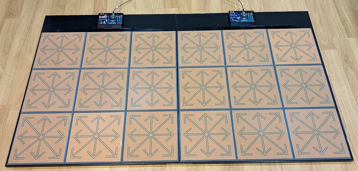
Two completed stages arranged side by side.
The final stage (1-player) is 34x40 inches and weighs 38 lbs (17.2 kg), though it feels heavier than this probably because there is no convenient way to hold it while lifting. The weight is heavy enough that placing the stage on a rubber-like liner on the floor keeps it from sliding around during active gameplay. Two of these stages are made to allow for doubles play; they are identical and connect to two USB ports on the host computer, where they show up as two joysticks and may be mapped accordingly in the game software. The spray painted and polyurethane sealed wood surface looks and feels more like a manufactured composite part than a wood part, which is the appearance I was trying to achieve. One change I would want in a future iteration is to make the controller board more flush with the top of the stage because presently it sticks out by about 0.5 inches above the level of the pads so the stages cannot be easily stacked, this would require a redesign of the controller board to use SMD components. There are no bolts or screws in this build - all components are held together with spray adhesive and hot glue - and so far I've had no cause for concern over mechanical rigidity. Gluing everything together means that components are not easily replaced, but there is little that can mechanically fail in this design. The uncoated FR4 surface of the 1-layer capacitive sensor PCB is used as the top contact surface which the player steps on. The frictional properties of this surface were found appropriate for gameplay, though it is slightly more slippery than a polycarbonate surface. It would be possible to glue a thin plastic sheet protector on top of the pad which would change the friction, but this did not seem necessary. The capacitance measurement was reliable and fast; in terms of the actual capacitance it is on the order of 0.1 nF and a change of about 20% between the non-contact and contact capacitance. There was no drift observed over time (so the live calibration feature is not even needed) and measurement noise is below 1% so contact can be reliably detected with just one sub-ms scan (given a well implemented ground plane - if there is not good contact of the stage with the floor, the noise increases and sensitivity decreases).
View from the front of the stage.
The audio mixer needs a major redesign; it was very susceptible to picking up noise and interference, and also it was not good at driving the audio output when loaded (which is not surprising given the filter capacitors and the ratings of the basic op-amp used). The feedback signal volume was too loud, and the resistor leading to the potentiometer (R20) should be increased perhaps to 100k ohms instead of 10k. The capacitor C10 should not be used as it causes high inrush current over the USB connection. Everything else worked as expected. So far I have played multiple days in dry winter air where static shock is a concern, and have not experienced any resets or false button activations.
View from near the floor, showing the thin profile of the stage.
In the center of the sensor PCB, where the grounded arrow lines intersect, there is about a 1 inch diameter area of low sensitivity. (I suspected this would happen, but did not have the inspiration to come up with a better design.) However this is only noticeable if you use the end of the heel or the tip of the toe to touch the pad right in the center, and this has never come up during actual gameplay. Otherwise the sensitivity and response is akin to that of a well tuned mechanical sensor system, with a much lower cost and maintenance requirement. The threshold and hysteresis can be easily adjusted in software to obtain a desired response. As mentioned before, this stage is not useable in shoes, but it is easily useable in socks and without requiring the player to be grounded (indeed if the bar is used, it should be isolated from ground so as to not change the sensitivity compared to not touching the bar). The absence of any deflection in the stage structure (unlike a mechanical sensor with a moving pad) means that the energy of a step or tap has to be absorbed by the foot - even though the displacement with a mechanical sensor is minor (1 mm or so) this difference can be felt in the impulse spectrum and requires slightly gentler motions. The capacitive sensor has a different type of sensitivity, so one may press down hard with a single toe and it will not activate, but pressing gently with a few toes will activate - surface area counts much more than downward force. Conversely, it is not possible to lightly rest the foot on the pad without activating it, so one has to be more explicit about releasing a button press. After a few hours to get used to the difference, there has been no impediment to rhythm game performance (at least with my style of gameplay). All 9 capacitive buttons work reliably, and the capacitance increase due to foot contact is effectively identical on all of them (the non-contact baseline differs and is stable over time). Pairing two (or more?) stages is easy and causes no interference in the capacitance measurement. Overall I would rate this concept a success.
For anyone who may be interested in a similar project, after a few months of using the above stage I would not suggest the capacitive approach, because the rigid structure and lack of deflection of the pads somehow detracts from the gameplay; stomping on the pads and using more rapid movements is unpleasant because of the rigid base, so I have to limit the force I apply which takes my focus away from the game. Perhaps haptic feedback is missing as well. Occasionally it is desirable to play in shoes for extra friction, which is not possible with capacitive sensing. Also having responsive LED lighting under the pads does make the experience more fun, and I've been missing it with the above design even though it doesn't change anything about the gameplay. I would recommend exploring inductive sensing, and making a pad where a tile with a layer of metal foil glued undeneath is placed on adhesive foam, with the foam allowing downward displacement of the tile (or perhaps a 3D printed flexure spring which allows downward motion but prevents lateral motion - see blowingstuff's build). Under the tile, a board containing an inductance sensor such as the LDC1614 is placed, and it senses the distance from the board to the conductive foil above. The speed, accuracy, and adjustability range of the LDC1614 is a good match for use in a rhythm game pad. After an initial build placing a separation of 5 mm to 10 mm between the metallic surface and the sensing coil, all other adjustments may be done in software, so no further mechanisms are needed. The LDC1614 supports 4 sensing coils, which may be placed on a square board that is slightly smaller than the tile itself, fitting underneath. With the foam spacers at the tile edges, this may be achieved without requiring any milling of the base surface.
A tricky part in getting started with a chip like the LDC1614 is the sensing board design, so I uploaded some files for a working board here in case anyone is interested. I use a spiral-like coil (made of slightly different semicircular arcs so not truly spiral) of 19 turns on each side of a 2-sided PCB that is 0.6 mm thick (the thinner board means the two layers of the coil are closer together, giving a higher Q value; it would also make for a thinner sensor to fit under the pad). The coil uses 0.127 mm wide traces, spaced 0.127 mm apart, which can be manufactured by most PCB suppliers today. The coil outer diameter is 19 mm. The coil design may be downloaded here as a DipTrace board (.dip file). Based on the TI webench coil designer tool, I use a 330 pF film capacitor to get a 1.8 MHz oscillation frequency, Q factor of 27, and 7 Kohm impedance. A board which contains two such coils and an LDC1612 may be downloaded here (.dip file). An Arduino-compatible code file (using the Wire library for I2C communication) to communicate with and configure the LDC1612 may be downloaded here. Test results when using the settings in the code, and placing a 6 mm thick piece of aluminum at various distances away from the coil, may be downloaded here. The test gives an estimate of both resolution and drive current to program at different separations. From the test results, I think there is plenty of resolution available to detect even light touches of the pad (0.1 mm displacement at 5 mm separation), and it should be possible to read all the sensors within 10 ms.