Physical interactions may be described by the concept of a field, a structure that defines scalar or vector quantities at each point in a spatial volume. While we can develop models and simulations of fields, typically our interactions with fields are indirect, limited by spatial, angular, or bandwidth constraints. The optical camera provides an example. The frequency of electromagnetic field oscillations in visible light is too high to measure directly, and the phase shifts between neighboring points is too subtle to measure directly. Therefore we use a lens and a camera, which set up a field coniguration inside the camera such that measuring the amplitude of oscillation across a 2D plane (the image sensor) provides information on the angular direction and distance from which different contributions to the field have originated. At the sensor we do not need to measure phase information, because the lens has already used this information to generate the 2D amplitude distribution at the sensor plane corresponding to angular direction of incoming light. In doing so - converting the field at the lens opening to a 2D amplitude plane - we take a particular snapshot, with a given orientation, field of view, and focal plane, which cannot be changed after the fact. If we were to capture more of the field, and in a more efficient manner (particularly involving phase), then it would be possible to adjust what was fixed in the snapshot, in effect applying any "virtual lens" of our choosing to create a 2D photograph after a "field image" has been obtained. There have been a few attempts to make an optical "field camera", such as Lytro in 2014, based on micro-lenses (in a sense, taking a photograph for what would otherwise be one pixel). In a sense the idea is still around today, with smartphones featuring multiple cameras which allow for software-aided changes in the focal plane. However this was largely not pursued commercially, because there is a lot of information in the optical field and it is difficult to capture a large fraction of this information while remaining competitive with a device that captures the information well at (effectively) a single point. Optical holograms are the closest thing we have presently to a field camera, and they demonstrate what is possible - one may use a conventional camera to capture a photo of a hologram from multiple angles or at different depth of field or using different lenses; the hologram encodes the information for a multitude of 2D photographs by accurately recreating the field over its entire surface. In a camera, light passes through a lens (point), and is incident on a sensor which gives a photograph; in a hologram there is no lens, and light is directly incident on the holographic sheet, which acts as sensor and later as generator of the field pattern.
While we still do not have the technology for easily deployable optical field cameras, in the realm of sound this goal should be more attainable. Due to the slower speed of sound relative to electrical signals, it should be possible to capture sound amplitude and phase in real time, thereby recording a more complete state of the acoustic field. As with the hologram, no lens is required to do so, which is an advantage with sound's long and varied wavelengths. There are commercially available microphone arrays, which have 10 to 100 microphones positioned a few cm apart and use software to determine the origin of sounds (ex1 ex2 ex3). There have also been individual projects of a similar nature (ex1 ex2). Likely the electronics you are using have microphone arrays for noise cancellation and directional amplification, such as amplifying sounds originating in front of the camera and attenuating sounds coming from the back. Then, what does this project seek to achieve? I wanted to make an acoustic field camera that could capture the sound level in a large volume, allowing for the main advantage of a field camera - virtual application of a lens, changing the field of view and depth of field, and further doing so in a manner similar to the pixels in an optical camera, with minimal reliance on phase-matching algorithms (which introduce diffraction-like limitations on the possible states of the field). This requires a physically large microphone array because of the long wavelength of sound, which would allow the recording of "sound movies" over a large area with multiple sound sources, something I have not seen done before. Consider that the eye's pupil, say 6 mm diameter, is about 10000 times larger than the wavelength of visible light; to capture this much of the field for sound at 1 KHz (0.3 m wavelength) would require a sensor that is 3 Km across! While such a large sensor is unrealistic, this comparison makes it clear that improving the image quality of an acoustic camera will require making the sensor as large as practical.
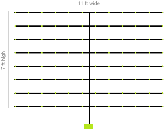
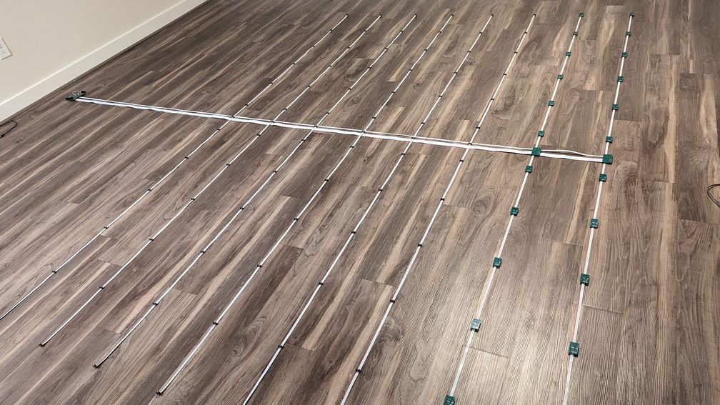
Proposed size (11 ft by 7 ft internal) and layout of a 96-microphone array for an acoustic camera to sense 100 Hz to 1 KHz.
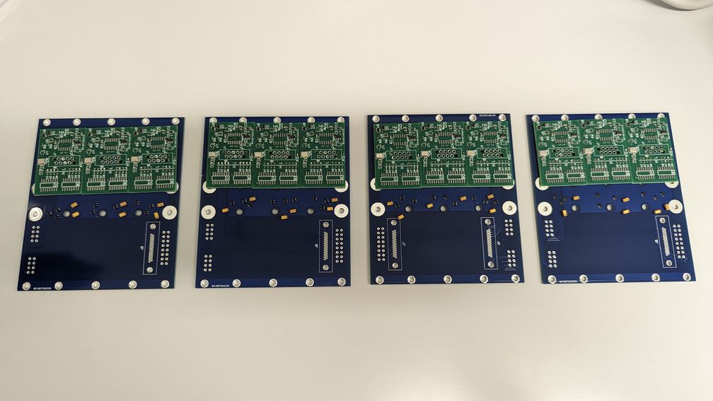
It is desired to maximize resolution, while maintaining a realistic sensor size. A concert hall might be 30 meters across, and with nominal 0.3 m microphone spacing, this would give a 100 microphone width, and with a similar height, a total of 10000 microphones. So I set out to design a system that is scalable to that number, though I will start out with a more modest (12 by 8) array of 96 microphones. If successful, such arrays could be built side by side, extending to (96 by 64) or any other desired multiple, to improve resolution. With so many microphones (in principle), it becomes important to minimize the cost of each sensor board, while still maintaining good sound quality. The long distances involved (multiple meters) make it very likely that analog signals will pick up noise, and also would require either individual ADCs or a carefully designed fast multiplexed ADC to digitize tens of incoming audio signals in rapid succession. To avoid these challenges, MEMS microphones which output an I2S digital signal (SDMO07C-26/1281) are chosen for the sensor boards. These may be read by a microprocessor and stored directly into memory as 16-bit samples, avoiding the need for FPGAs or DSP routines to reconstruct a PDM signal.
The sensor boards send their data onto a common bus with time division multiplexing, allowing 12 microphones to share a bus (the microphones on either end of the bus terminate the differential lines with a resistor). This data is received by an intermediate board. Eight of these intermediate boards send data in parallel to the receiver board, which supplies the clock, records the 96 microphone channels, and carries out data processing. The buses use M-LVDS, which is a (relatively) low power differential signaling protocol, expected to reduce EMI and improve signal quality given the long unshielded ribbon cable that will be used to connect all the boards. The ICs used for MLVDS are two SN65MLVD048 quad-channel receivers on the receiver board, and SN65MLVD205A full duplex receiver / transmitter on the intermediate and microphone boards to simultaneously receive the clock signal and transmit the audio data. The SN65MLVD048 is configured for Type-2 operation (and the SN65MLVD205A is hard-wired for Type-2 operation) which means that when the shared bus is not driven by any transmitters, the receiver will see a well-defined zero state, which is used as a way to verify microphone synchronization with a "silent bit" between when one microphone stops transmitting and when the next microphone starts.
The receiver board also supplies the power for the whole system. Most of this power is used by the differential transmitters and receivers, one for each microphone and two for each intermediate board. The power to the receiver board is supplied using Power over Ethernet (PoE), with the voltage isolation and conversion done by the module Ag9205-S (capable of supplying 13 W). This decision was important for the future scalability of the system, because it means only one cable needs to be connected to each receiver board, and this cable may be tens of meters long without worrying about resistance losses (because of the higher transmission voltage (50 V) which is then converted down to 5 V locally at each receiver board). A similar approach is used from the receiver board to the microphones, where a 5 V line is used for distribution, and each microphone has its own 3.3 V LDO regulator (TC1014-3.3), so that resistive voltage drop in the wires does not affect the performance of the sensor boards. PoE switches may be readily purchased and networked together, so if some day I decide to operate multiple sets of these arrays, it will be straightforward to do so. Common PoE switches can supply enough power to guarantee 12 W received by each powered device (and negotiating higher powers over PoE becomes an interface challenge in itself), so the power budget for this system is 12 W. An I2C voltage and current meter (INA232 with 0.030 ohm resistor) was used to monitor the power draw of the system, which was a very useful addition to confirm everything is functioning as intended. A load switch with integrated discharge resistor (SiP32509, verified during receiver board testing to handle 2 A continuously) was used to allow for software powering on/off the microphone array 5 V supply, as well as controlled charging and discharging of the array capacitance. On each microphone and intermediate board there is a 10 uF tantalum capacitor at the 5 V input, another 10 uF tantalum capacitor at the 3.3 V regulated output, and a few 0.1 uF, 4.9 nF, and 470 pF capacitors at different IC pins. A shutdown signal powers off all 3.3 V regulators in the array when it is pulled low, and allows for progressive start-up. Additionally, this signal is used to sense the number of microphones: a 100 Kohm resistor is connected between the shutdown line and the 5 V rail on each microphone board, so that when the shutdown line is pulled low, the current in it is proportional to the number of microphones with approximately 50 uA per microphone. This gives a confirmation that at least some of the pins on the connectors are functioning properly and could help with debugging (there were no issues encountered with this approach; to measure the current a second INA232 with a 15 ohm sense resistor was used).
The high speed bit clock and data are transmitted using low voltage differential signaling, which was an expensive but worthwhile choice for the multiple-meter scale of this project because it is quite robust to electrical interference (even then, errors may be introduced with improper handling). The reset line, which synchronizes timing across the array, is not differential because ideally it would only be used once at the start of the acquisition. For the intended application of a few minutes continuous runtime, this was sufficient (over hours, perhaps something would become desynchronized, but I haven't seen that happen unless the system somehow receives a large burst of electrical noise). The shutdown line needs to, when powered on, always exceed the minimum threshold voltage from the LDO regulator datasheet, even in the presence of 0 V potential shift due to current in the 0 V wires, and in the presence of noise spikes coupled from nearby high speed wires - otherwise a microphone board may randomly power down, which would throw the entire microphone bus out of synchronization. The reset line similarly needs to remain above or below some defined threshold even with noise present to avoid randomly resetting the synchronization of a microphone board. While the shutdown line does not have any stringent timing requirements (because it will just remain on for the entirety of data collection), the reset line should maintain a decent rising and falling edge. For this, I use inverters with Schmitt trigger input (74AHC1G14 and 74LVC1G14 for higher current) at the receiver board, intermediate boards, and microphone boards. This acts as a buffer and cleans up the signal (improving the rising edge) as it propagates down the wire. The receiver board emits an inverted reset signal that is inverted, then inverted again at each intermediate board, then inverted again at each microphone board. This appears to work as expected in synchronizing the microphone boards to the bit clock. The inverters are specified to handle a voltage at the input even with their Vin pins at zero potential, which may occur if the external 5 V bus is powered off but the receiver board emits a low reset signal (which is inverted to high). All the other components are also confirmed to handle such edge cases of various rails being switched on and off (the LDO regulators can handle a positive voltage on the shutdown pin with zero Vin, the INA232 can handle a positive voltage on the sense resistor with zero Vin, the load switch can handle a positive voltage on the switch input pin with zero Vin, the MLVDS receiver can handle a positive voltage on the receive pins with zero Vin) as well as components being plugged or unplugged (the system is not designed to be altered when powered on, but will not be destroyed if that happens). Some other circumstances include the Teensy being powered from USB 5 V in the absence of 5 V from PoE, and the Teensy being removed from the receiver board in the presence of 5 V from PoE.
The data is carried from microphones to receiver board using 1.27 mm pitch 28 AWG ribbon cable. The time-division shared buses use a 8 conductor wide cable (0 V, 5 V, Shutdown, Reset, Clock-, Clock+, Data-, Data+). The parallel buses use a 20 conductor wide cable (Clock-, Clock+, 8x(Data-, Data+), Shutdown, Reset) in parallel with a 8 conductor wide cable (4x(0 V, 5 V)). The resistance of the cables carrying 0 V and 5 V power (including resistance of the 8-pin connectors) was modeled in CircuitLab with maximum and nominal power draw conditions, and the voltage drop from 5 V at the receiver board to the furthest away microphones was confirmed to be within the operational limit of the 3.3 V LDO regulator, therefore the regulated voltage is expected to be a stable 3.3 V despite varying power draw of the microphone array. In the presence of large current flows, the 0 V at distant microphones is expected to be at a higher potential than 0 V at the intermediate and receiver boards, and all the signal lines are confirmed to be operational under this condition (the high speed differential signals can handle this easily, while the single-ended reset and shutdown signals need to be checked against IC switching limits specified in their datasheets).
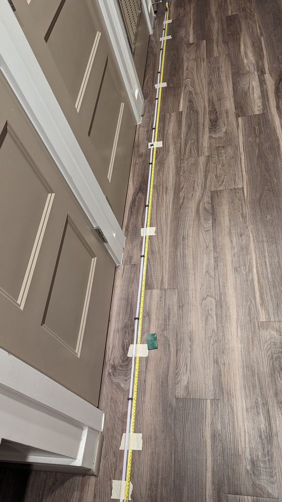
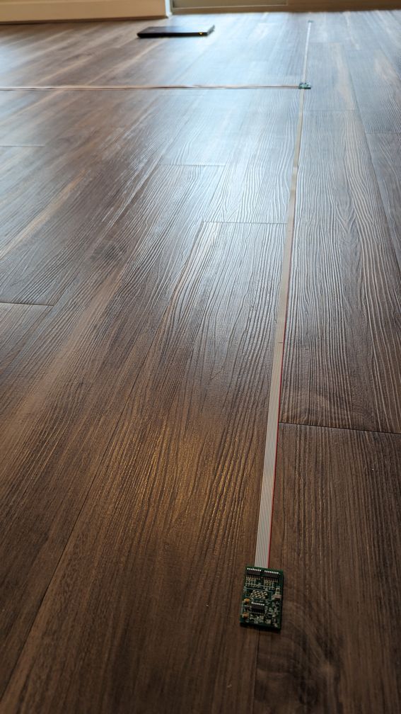
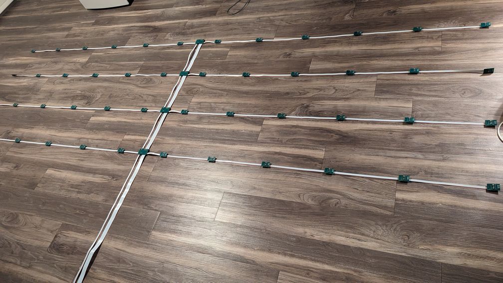
The ribbon cable is laid out next to a measuring tape. Both are taped to the floor (with low adhesion painter's tape) for improved consistency in the connector location on different cables. Assuming we can resolve sound phase to 1 part in 100, the spacing tolerance at 1 KHz is 3 mm. The crimp-on connectors are spaced using the measuring tape, and crimped in place using a stack of PCBs (seen towards the bottom of the photo).
The use of ribbon cable and shared bus lines was chosen so that all connections could be made using crimp-on connectors (Wurth REDFIT, parts 490107670812 and 490107672012) which mate directly to the PCB with through-holes. This eliminates the need for soldering or cutting wires (as may be required for daisy-chaining), which in a project of this scale will rapidly become an annoyance. Still, crimping these connectors was not "a breeze"; they require quite a bit of force (80 kgf on the 20-wire cable) to fully attach on the ribbon cable since they are displacing the insulation in the process. Apparently there are special crimping tools for this but I could not readily find one, so I had to use a less elegant approach. To attach the connectors without breaking the pins or the plastic case (which would happen if using pliers), I used hot glue to join three intermediate boards stacked on top of each other, which had the correct hole patterns for the 8-pin and 20-pin connectors, and the increased thickness of this assembly would provide a flat surface which can be compressed against the back surface of the connector. At first I did not use enough force (just pressing down with my hands) and the connections were unreliable, however after compressing them fully (using body weight), I did not have any problems with electrical connectivity in the approximately 1000 pins that resulted.
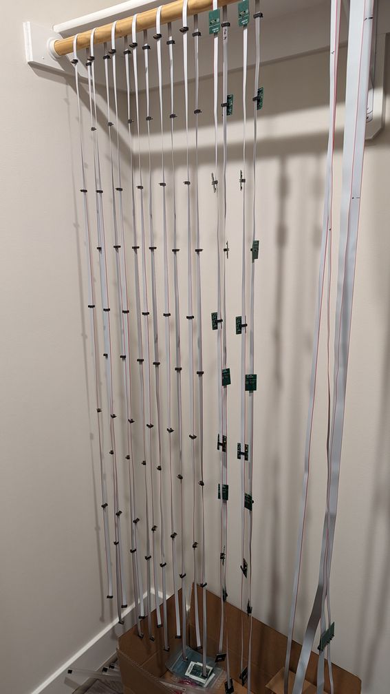
Storage of all the long cables becomes a concern in a studio apartment - here the cables are shown hanging in a closet.
I started with a proof of concept using just two microphones on the farthest ends of the cabling, which would confirm that the differential signal can be transmitted reliably on ribbon cable over a few meters of distance. This would also test other aspects of the system such as power supply and data collection, without the risk and complexity of extra microphones in the circuit. The electrical aspects of the test were successful; on the software side a few errors had to be addressed which are discussed in the software section. (Since I placed the crimp connectors on either end of the cable to do this test, all the other connectors which would go in between had to be taken apart and put back together around the cable rather than slid on, but this was a minor inconvenience.)
Laying out two microphones and associated ribbon cables on the floor. Because the outer dimensions are relatively large, the circuit boards are a bit difficult to see in a photo of the entire system. A laptop is placed on the floor near the top of the photographs for a sense of scale.
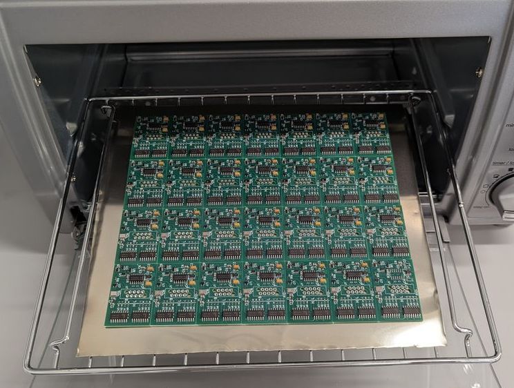
Next it was time to scale up. I set up a stencil to deposit solder paste on each microphone board, then I placed the components and heated the boards in a toaster oven to solder everything together. Since the small microphone boards had components extending to the board edges, I would place 3 microphone boards together onto a larger board which could be more easily handled. Small surface mount components, which were delivered in a tape designed for pick and place machines (I guess I am the machine this time), were sorted and placed onto the larger boards adjacent to the microphone boards, working on one larger board at a time. Then I could manually place each component with reduced risk of an accidental hand motion causing a loss of components or boards. One problem that became apparent was that the stencil openings for the annular region around the microphone opening hole (which is also the electrical 0 V connection) was too small. In DipTrace I had defined the microphone pattern using a through-hole for the opening (which does not have a solder paste region associated), and arcs drawn in the solder paste layer overlapping the through-hole annular ring were used to define the holes in the solder paste stencil. The width of these arcs was insufficient, so I manually added solder paste in this area on each board.
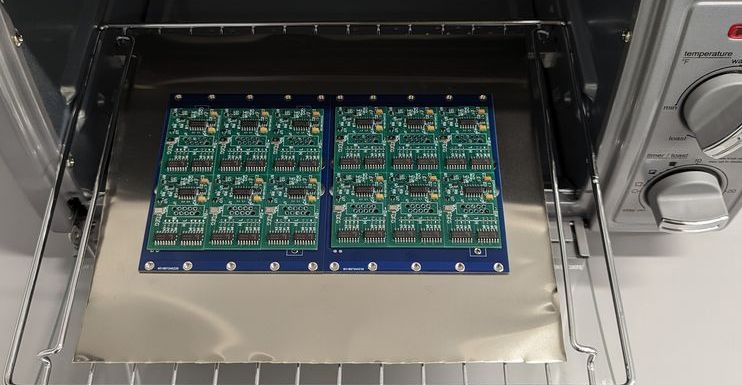
Components are placed on larger boards that act as trays to hold three microphone boards at a time. This improves handling and reduces the impact of errors. 12 microphone boards at a time are heated up in a toaster oven to melt the solder.
The boards were baked, 12 at a time, in a toaster oven (with advertised "even toast" technology!) with a thermocouple probe used to read the temperature. Placing the thermocouple was a bit tricky because it would have to be done without disturbing the carefully placed components on the PCBs, while still ensuring good contact to a metal surface (the tip of the thermocouple would be placed to fit inside one of the holes for the 8-pin connectors, with the weight of the thermocouple wire providing sufficient downward force to achieve thermal contact). The oven would be turned on at full power ("toast mode", 1200 W or so, with both top and bottom heating elements active), then once the thermocouple reads 210 degC (for leaded solder, 245 degC for leadless), the oven would be turned off; the heat capacity of the interior of the oven would provide about 30 seconds soak period above 210 degC, then once the temperature dropped below 180 degC the door is opened and a fan is used to cool down the boards. A thick layer of steel foil was placed underneath the boards, and a thick steel tray was placed above, in order to spread the heat more evenly and promote more heat transfer by convection and conduction instead of radiation. With a single layer of PCBs this arrangement gives a temperature profile that is surprisingly close to the recommended one for most solder pastes - slightly slower (1.5 x duration) on the heat-up and a lot slower (4 x duration) on the cool-down (unless the door is opened and a fan is used as described). Because I placed the microphone boards on top of the larger "tray" boards, the heat-up took close to 5 minutes, which is not good in a toaster oven as the temperatures on the top of the surface mount components may become substantially hotter than the bulk PCB due to the radiant mode of heat transfer depositing its energy only in the outermost micrometers of material. Indeed the ICs and tantalum capacitors looked a little bit charred, especially at the back of the oven which was farthest away from the door and slight opening through which the thermocouple (and room temperature air) entered.
There were no problems seen during optical inspection following the reflow process, other than small solder balls near some components and particularly on the sides of SMD capacitors; these solder balls were affixed securely in the solidifed residue of the "no-clean" solder paste, and had no impact on the electrical performance. Because the residue layer was insulating and held the balls in place, there was no incentive to remove the balls. I tried a few variations on the temperature profile (as much as a manually controlled toaster oven would allow) and solder paste thickness and solder paste type, however nothing seemed to eliminate the formation of small solder balls or to be conclusively associated with it. If using a water washable solder paste, the balls could be washed away in a water cleaning followed by drying under a compressed air stream, but this leaves the board in a bare uninsulated state compared to the thin insulating layer formed with the "no-clean" paste, so I kept the process unchanged. I did not like that with the SMD microphones all pads were underneath the body of the device and thus impossible to inspect optically, however by the end of the project there had been no issues attributable to poor connections on these pads. Each batch of 12 microphones took about 4 hours to complete.
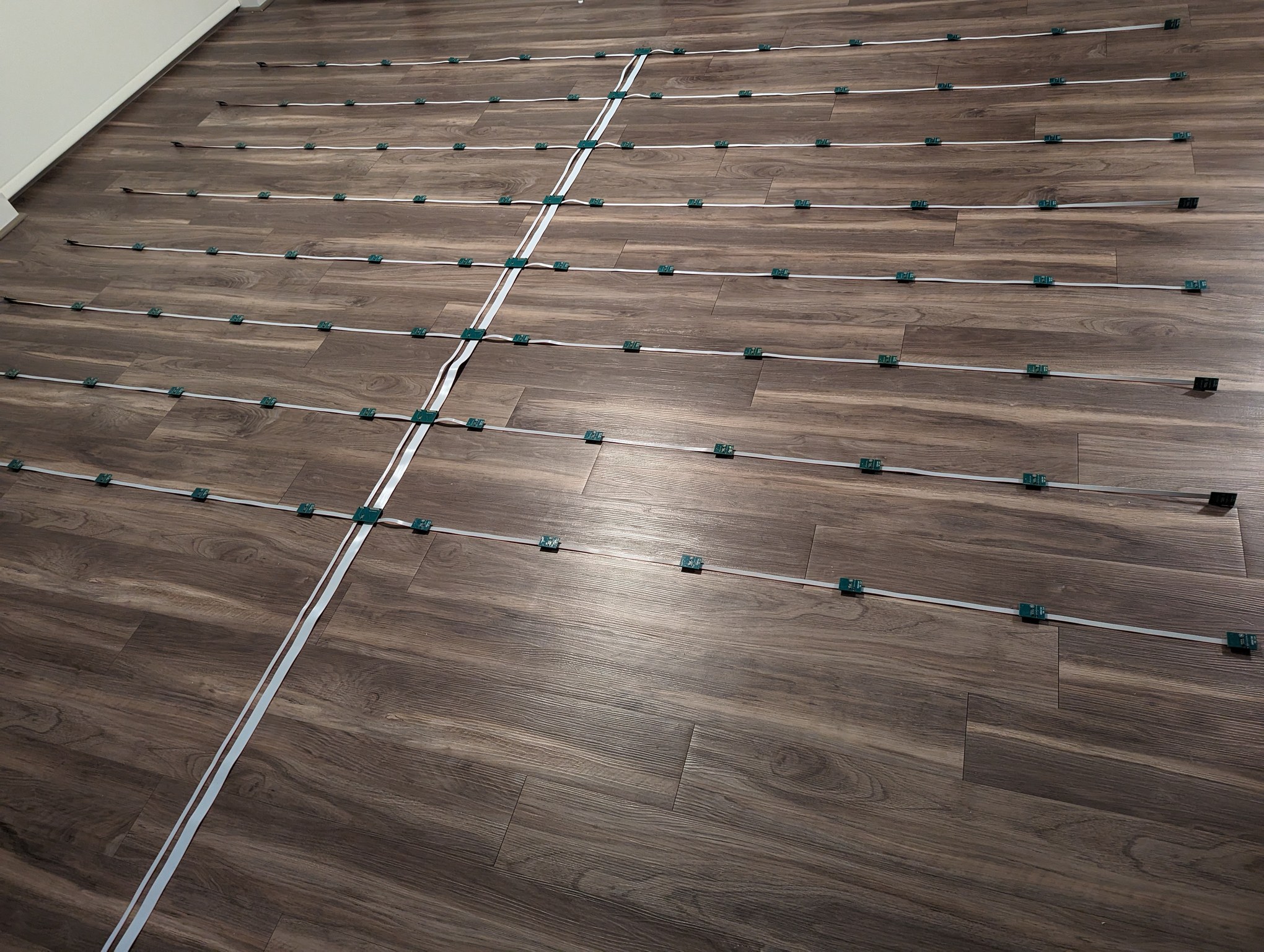
Laying out 24 microphones (2 buses) and all other (6 buses) ribbon cables on the floor; two perspectives are shown with the second including the receiver board towards upper left of photograph.
Testing the 24 microphone system, problems started to become apparent. The parallel bus shared between 12 microphone boards necessitates that all the boards are synchronized, and remain synchronized during data acquisition. Each board has its own 8-bit counter (based on two MC74HC161 4-bit presettable counters) which tells it when to start and stop transmitting on the bus, and when all are properly synchronized, they maintain a phase offset (defined by soldered jumpers on each board, with the reasoning behind jumper positions described here) which allows each board to transmit during a defined time slot when all others are silent. There were a few clocks which had to be considered in this design, given a sample rate SR:
The strategy is that BCLK is transmitted out to all the microphone boards, and then each board has its own 8-bit (256-step) counters to generate WS and SCK. When the reset line is activated, the counters are pre-loaded to a unique value for each board on a shared bus, and then if they all stay synchronized, each microphone transmits during its "own" time slot. The counters are set up such that transmission to the bus begins synchronized with its local WS falling edge. The SDMO07C-26/1281 microphones used here transmit for 24 of 32 bits and are in a high impedance state the rest of the time, however audio data is only in the first 18 of the 24 bits with the rest output as 0. A 100 Kohm pull-up resistor is connected so that a 1 is received when the microphone is high-impedance, and a type-2 MLVDS receiver is used so that a 0 is received when the bus is idle. 21 bits (of 256 per counter cycle) are available for each microphone, of which the first bit is defined as 1 (this is the LSB of the right channel, which means the left microphone is high impedance and the pull-up resistor results in a 1), the next 18 bits are the audio data, the next bit is defined as 0 (per the microphone datasheet), at this point the board stops transmitting and the next bit is also 0 because the bus is idle. There are also 4 bits left over in the counter cycle with 12 microphones (21*12+4=256) which are defined as 0 because the bus is idle then (no board transmitting). All of the defined values may be used by the receiver board as a way to check that synchronization is being maintained during data acquisition.
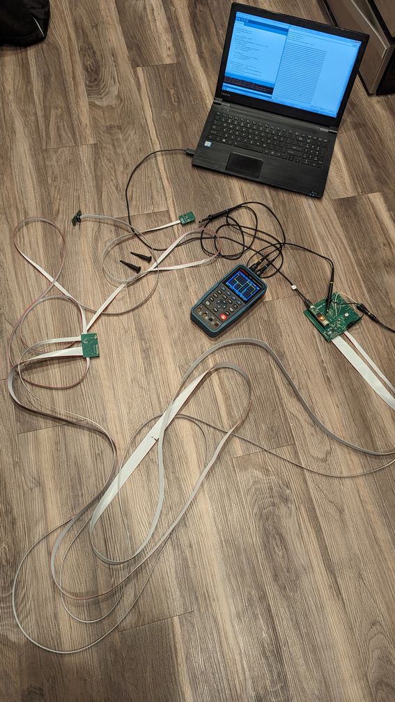
A laptop and portable oscilloscope are used to debug the microphone data transmission (this is an earlier photo showing the 2 microphone, rather than 24 microphone, arrangement). If you look closely, the rising and falling edges of the yellow oscilloscope trace represent the start of a 256-bit transmission cycle, while the rising and falling edges of the blue trace represent the start and end of one microphone's 20-bit transmission within that cycle. This version of the receiver board is powered from a regular barrel connector power supply instead of PoE.
Unfortunately, with 24 microphones, the system would regularly fail the synchronization check. I used a surprisingly-capable 2 channel portable oscilloscope from amazon, along with a "slow mode" routine that would output a 1 KHz rather than 2.5 MHz BCLK (the microphones are in a "low power" mode and remain high impedance through the entire transmission window, so instead of 18 bits of audio data I would expect a stream of 18 1s due to the pull-up resistor), to troubleshoot the clock signals. The failure mode was odd - in slow speed testing, the boards would end transmission randomly but begin transmission at the appropriate time, mostly. This meant that the counters were staying synchronized, but for some reason the logic to begin and end transmission based on the counter value was faulty. The last IC in the chain sending the transmit enable signal is a D-type flip flop (SN74LVC1G175), which is set by a rising edge of the counter MSB on the clock pin, and reset by a condition that occurs 20 bits subsequent. Because both of these are edges (rather than steady values), the output would be affected by high frequency spikes especially on the reset line, because after a reset the output would remain low until the next clock rising edge. This is indeed what was happening - the counters remained synchronized and the rest of the logic ICs somehow handled the electrical noise, but the flip flop would readily trigger and reset on the noise, making bus transmission unpredictable. I connected a 470 pF capacitor (because that's what I had laying around, a smaller value may have worked as well) on the clock and reset pins of the flip flop, positioned immediately adjacent to the pins, and this resolved the issue. With all 24 microphone boards modified in this way, the boards transmitted audio data as expected and remained synchronized for the entire duration of 4 minute tests.
Synchronization would be lost if I tried grabbing and moving the ribbon cables, probably because the change in impedance due to the added capacitance with my hand when grabbing the cable caused enough high frequency noise on the lines to throw off some of the boards. Indeed, seeing the amount of noise nominally on the wires with the system working properly speaks to the importance of using differential signaling, and I felt relieved that I picked MLVDS due to this robustness - a project of this scale would be a major EMI headache if trying to use single-ended signaling. One change I wish I could make is the use of slower MLVDS ICs (I didn't find any) because BCLK here is at most 3 MHz while the MLVDS ICs used are capable of 100 x that, which means they are susceptible to receiving and emitting high frequency spikes which serve no purpose in this system. However, this relatively slow rate also means reduced power draw of the ICs, which allowed the microphone array to be substantially under the 12 W power budget (more details below).
To avoid more manual work on the remainder of the microphone array, I ordered a new stencil (with larger holes for the microphone annular pad), new microphone boards (including the two 470 pF capacitors mentioned above), and new receiver board. The receiver board was a silly mistake - I oriented the ethernet jack so it was facing backwards, because I assumed the pins for the LEDs were at the front of the jack as that's where the lights appear - in fact the LEDs were at the back of the jack and transparent plastic tubes were used to transmit the light to the front. In addition I improved the ground plane around the single-ended signal traces between the MLVDS receivers and the Teensy 4.1, and relocated the microphone timing reset signal to a Teensy pin which could be driven by FlexIO (details in software section). The intermediate boards and terminating boards would have the MLVDS termination resistors replaced from 100 ohms which I ordered as a nominal value to 170 ohms which was specified in the ribbon cable datasheet as the balanced impedance, even though the 100 ohm version (unbalanced impedance) seemed to work just as well and oscilloscope traces of the signals didn't seem to change much. On the microphone boards I also switched to U2J instead of X7R for the 0.1 uF capacitors, to avoid a possible piezoelectric effect (in this case, fluctuations in voltage causing vibration of the capacitors which would be picked up by the microphones acoustically) because there seemed to be strange high frequency noise in the audio data when listening back to recordings. This noise (acoustic source) is easily distinguishable from electrical interference noise because the audio is transmitted digitally from the microphone boards - electrical interference sounds more glitchy, random, and like loud white noise, while acoustic noise has a well defined frequency and sounds softer. The 470 pF and 4 nF capacitors were already C0G which is not piezoelectric. A few weeks later I noticed that the high frequency audible noise went away when passing the audio data through a high-pass (rather than low-pass) filter: in fact the noise was coming from my computer's sound card trying to recreate a static non-zero output (DC offset) because the raw microphone data is not centered on zero; when the data is properly centered (removing the components under 20 Hz) the noise goes away and the microphones are confirmed to work quite well with clear sound coming through. All that said, there does not seem to be any piezoelectric issue with using the X7R capacitors for power bypass on the microphone boards.
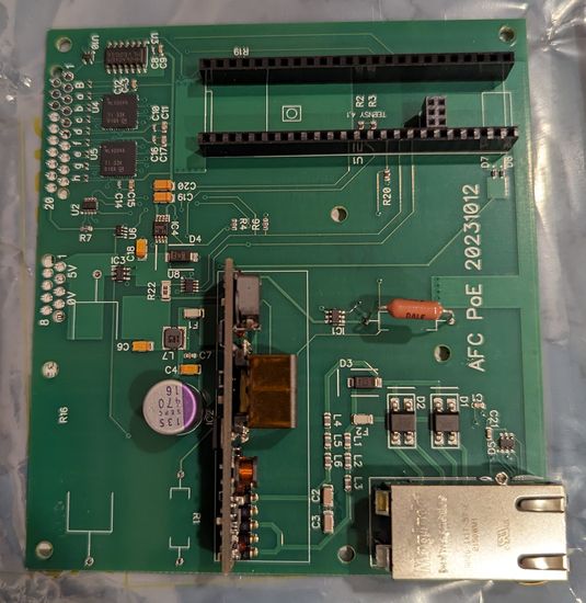
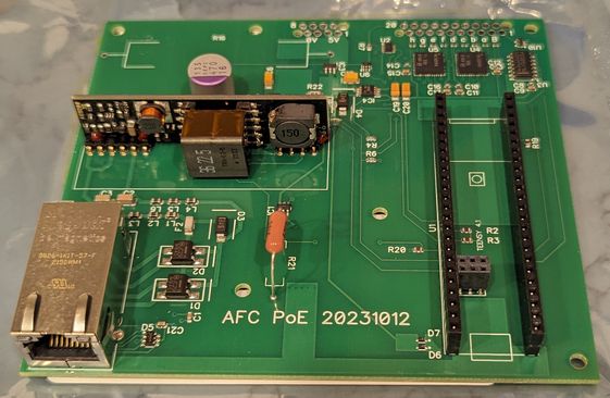
Two photos of the receiver board with ethernet jack, PoE module, and the 8-pin and 20-pin microphone array connectors with MLVDS receivers and transmitter nearby. A Teensy 4.1 board with ethernet chip is placed in the header sockets (the 6-pin ethernet connection is made with parts M22-2020346 and SQT-103-03-L-D). There is also space for a large 15 W resistor which was used to test the power capacity of the receiver board up to the 12 W power budget prior to connecting the microphone array. The through-hole resistor visible on the board is used to ensure a minimum 200 mA is drawn from the PoE module, to support the module's voltage regulation and also possible requirements by the PoE switch to have a minimum load to avoid cutting off power. In testing, it turns out the Teensy 4.1 draws a bit under 200 mA from the 5 V rail when powered on, so this resistor is unnecessary.
In the next round of microphone board assembly, I optimized the process slightly. I still used "trays" containing 3 boards each, but now worked on 24 boards (8 trays) at a time instead of 12. I also placed more parts at once; previously I would unpack 1 or 2 ICs per each board, place all of them, then unpack the next ICs. This time I would unpack between 8 and 10 ICs in each step, with each step having ICs that look sufficiently different to avoid mix-ups. This reduced the number of interruptions in the placement process. Also it reduced the mental load, because I could repeat the same set of actions 24 times in a row instead of regularly thinking about where new components should be placed. With this, I was able to double my throughput to 24 boards per 4 hours.
Baking 28 microphone boards at a time, directly on a steel foil surface to reduce heat capacity and improve heat conduction.
This time I placed the microphone boards directly on the steel foil in the toaster oven, which reduced the heat-up time and gave a better match to the recommended temperature profile for the solder paste. I then tested audio capture with the new batch of 24 microphones and the previous 24, a total of 48 and half of the design goal.
A test with 48 microphone boards and 4 intermediate boards.
All 48 microphones worked and stayed synchronized for the duration of the test (10 minutes). Then I used the same approach to complete the remaining 48 microphone boards, which were also confirmed to function as expected. The PoE module worked successfully to supply power to the microphone array from a single ethernet cable. The DipTrace files (schematic and board design) for the final version of the microphone, intermediate, and receiver boards may be downloaded here.
The receiver board needs to supply power to the microphone array, generate the ~2.5 MHz BCLK differential signal along with timing synchronization signal, receive audio data on 8 parallel differential lines, then process and write out the audio data to an SD card. It also needs to receive and respond to basic commands over ethernet, and at some point for future expansion it would need to receive Precision Time Protocol frames over ethernet to synchronize timing between multiple arrays (this is not implemented at present, but could be, as the IMXRT1060 chip on the Teensy 4.1 has hardware support for IEEE 1588 in the ENET module).
Mostly the above is a passive operation, in that the receiver board doesn't care about the data coming through. This is complicated by two factors: it would be useful to verify synchronization by checking the values of certain bits as described above and try to recover from synchronization errors, and it is also necessary to buffer up to some 150 ms of data because writing to an SD card may incur an unpredictable delay. Despite the occurrence of this delay, the audio data stream must be acquired continuously at the BCLK rate. Therefore the data acquisition must be implemented with non-blocking code.
The timing and bit shifting associated with BCLK and audio data are handled by the FlexIO module of the IMXRT1060. This module is a good match for the application requirements: it has 8 timers and 8 shift registers which can be driven by these timers. The FlexIO module ranks high on the metric {module functionality} / {length of description in datasheet}, so it took me a while to figure out how to properly configure the module. Timer1 was used to generate the BCLK signal and output it to a pin, then shift registers 0-7 were used to shift in one bit from each of 8 data input pins on the falling edge of Timer1. FlexIO3 was used because the Teensy 4.1 PCB layout exposes 8 FlexIO3 pins on one end of the board. The FlexIO module is configured as follows:
CCM_CCGR3 |= CCM_CCGR3_FLEXIO2(CCM_CCGR_ON); //sends clock to FlexIO 2 and 3

FLEXIO3_CTRL |= 1; //enable FlexIO3IOMUXC_SW_MUX_CTL_PAD_GPIO_AD_B1_05 = 9; // Bus a - HW pin 41 to FlexIO3.05//Shift data in to buffers, SHIFT0 for bus a to SHIFT7 for bus h
FLEXIO3_SHIFTCTL0 = FLEXIO_SHIFTCTL_TIMSEL(1) | FLEXIO_SHIFTCTL_TIMPOL | FLEXIO_SHIFTCTL_PINSEL(5) | FLEXIO_SHIFTCTL_SMOD(1); //shift on falling edge of TIMER1 from pin f5FLEXIO3_TIMCFG1 = FLEXIO_TIMCFG_TIMOUT(1) | FLEXIO_TIMCFG_TIMDEC(0); //run timer indefinitely, from FlexIO clock
FLEXIO3_TIMCTL1 = FLEXIO_TIMCTL_TRGSRC | FLEXIO_TIMCTL_PINCFG(3) | FLEXIO_TIMCTL_PINSEL(16) | FLEXIO_TIMCTL_TIMOD(1); //operate in dual 8-bit baud mode, internal trigger (not used), and output to pin f16FLEXIO3_TIMCMP1 = 0x3F05; //baud divisor of 12 (30/12=2.5 MHz) (12/2-1=0x05), 32 bits (32*2-1=0x3F)attachInterruptVector(IRQ_FLEXIO3, &dataInIRQ);IOMUXC_SW_MUX_CTL_PAD_GPIO_B1_00 = 9; // BCLK - HW pin 8 to FlexIO3.16
delay(100); //wait for microphones to receive BCLK and start converting data
FLEXIO3_SHIFTSTAT=0xFF; //clear status flag
while(!(FLEXIO3_SHIFTSTAT & 0x40) && stall_ctr < 100000){ stall_ctr++; }
FLEXIO3_TIMSTAT=0xFF; //clear status flag
digitalWriteFast(pin_reset_inv, HIGH); //reset signal low at microphone boards (driven through inverters)
while(!(FLEXIO3_TIMSTAT & 0x02) && stall_ctr < 100000){ stall_ctr++; } //wait until next buffer is read (32nd falling edge)
digitalWriteFast(pin_reset_inv, LOW); //reset signal high at microphone boards (driven through inverters)
FLEXIO3_SHIFTSTAT=0xFF; //clear status flag

  FLEXIO3_SHIFTERR=0xFF; //clear overrun error flags

  NVIC_ENABLE_IRQ(IRQ_FLEXIO3);//enable interrupt

FLEXIO3_SHIFTSIEN=0x80; //enable interrupt on SHIFT7 fullif(FLEXIO3_SHIFTERR != 0){ //overrun error - we are likely desynchronized on wordInNum now
sr_ovr_errors++; FLEXIO3_SHIFTERR = 0xFF; //reset error flags
}
if(FLEXIO3_SHIFTSTAT != 0xFF){ //expect all buffers to be filled
rb_write_errors++; //flag will be reset by reading shift register
}
wordInNum=(wordInNum+1)%8; //keep track of 8 32-bit shifts for a 256-bit cycle
micReceiveBuf[micReceiveWrite]=FLEXIO3_SHIFTBUFBIS0; //read MSB-first data, buses a-hFLEXIO3_SHIFTSIEN=0x00; //disable shift register interrupts
NVIC_DISABLE_IRQ(IRQ_FLEXIO3);
IOMUXC_SW_MUX_CTL_PAD_GPIO_B1_00 = 5; // BCLK - HW pin 8 to GPIO
digitalWrite(8, LOW);Once (8x parallel) 32 bits are shifted in, an interrupt routine would place the unprocessed data into a 397 KB circular buffer, making liberal use of the IMXRT1060's 1024 KB RAM to have a buffer large enough for 150 ms of data at a combined ~20 Mbit/s. Another non-interrupt routine would reconstruct the 32-bit data chunks into 256-bit chunks for each microphone bus by combining 8 subsequent 32-bit values, then it would verify synchronization is maintained, and in that case transfer the data to another 32 KB circular buffer (RingBuf.h of SdFat library) which would contain data in the format for writing to the SD card (unnecessary bits removed). Another routine would check if the SD card (using the SdFat library) is free (if(!file.isBusy())) to accept more data and at least 512 bytes are available to write, in which case data would be written to the SD card 512 bytes at a time. The SdFat library's ring buffer function rb.writeOut(512) is non-blocking if called when the SD card is free, however if called when the SD card is busy, the rest of the code hangs until the SD card is free again. By checking file.isBusy() beforehand, the data processing and storing in circular buffer routines are able to keep operating with minimal time penalty (16 us) even if the SD card itself requires a delay during the write. With this approach, I have not had problems with data integrity or synchronization over multiple minutes of acquisition. A fast SD card is necessary - SD cards were seen to differ in terms of write speed, and this affects the maximum delay time as well as the average data rate. I used a 1 GB SanDisk card which was confirmed (using the Benchmark example in the SdFat Arduino Library installation) to give an average of 4 MB/s write speed. I found that there are effectively no delays when writing to a pre-allocated new file on a new card. However if a file is deleted or overwritten, then writing new data even with pre-allocation incurs random delays of a few ms duration, perhaps because the SD controller has to erase the previously stored bits.
In addition to receiving commands over a USB serial connection, the controller can receive commands over ethernet. For this the QNEthernet library is used, which handles the requirements of establishing a TCP/IP connection. Within the main loop, a call to EthernetClient client = server.accept() accepts an incoming connection if one is available, and data is sent back in HTTP/1.1 format. A GET request coming from the client can be used to set parameters such as the filename and to begin or stop data acquisition. The controller responds back with a plaintext webpage that indicates the status of the microphone array. Without any optimization beyond basically copying the QNEthernet server example, this was seen to not cause errors in data processing rate or synchronization, even if rapidly pressing the refresh button on the client browser or unplugging and plugging in the ethernet cable on the client side while data collection is ongoing. Note that this was not the case with the Teensy USB serial output, where calling Serial.print() with a long string (hundreds of characters) would likely cause a data synchronization error. Perhaps this is because the serial output function has to wait for the next USB poll cycle (every 1 ms) if the serial buffer is full.
The firmware code may be downloaded as one huge (over 1000 lines) .ino file here. The code for the ethernet server is just an interspersed pasted copy from one of the QNEthernet examples, which will be easy to tell from the differences in code style.
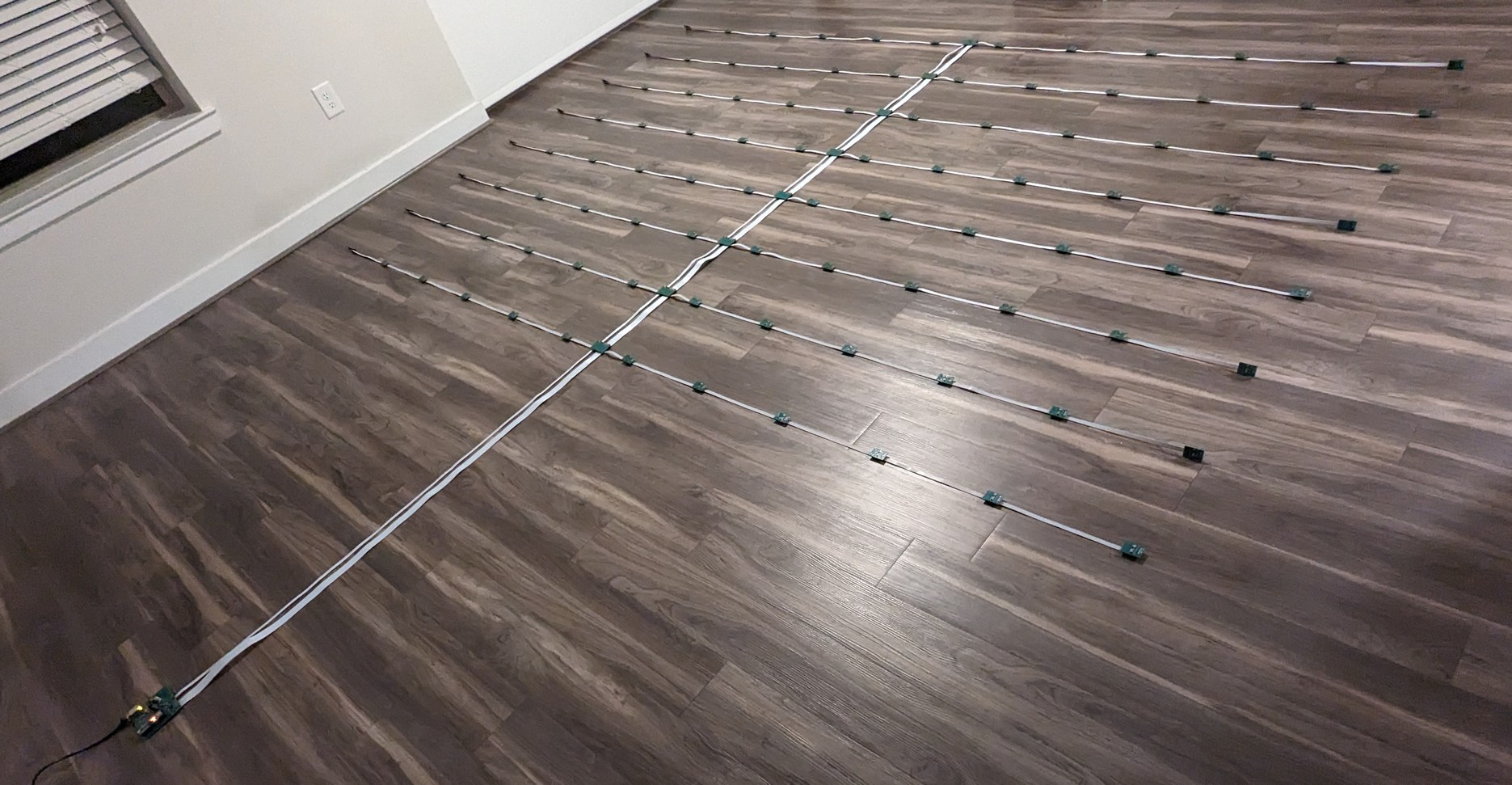
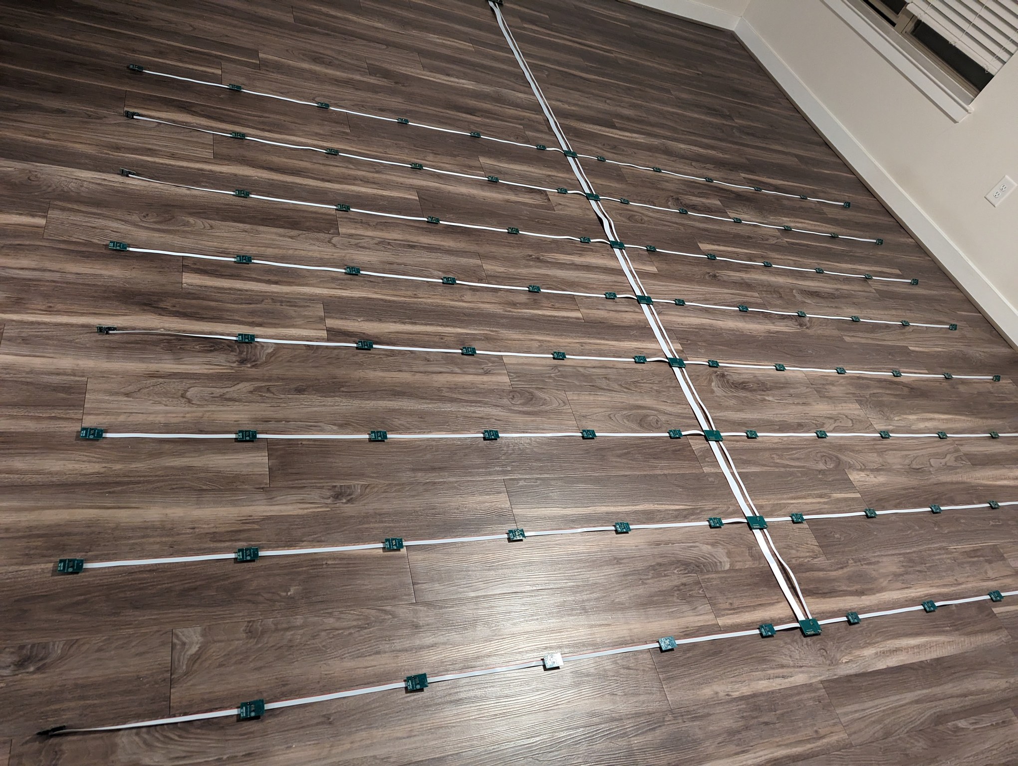
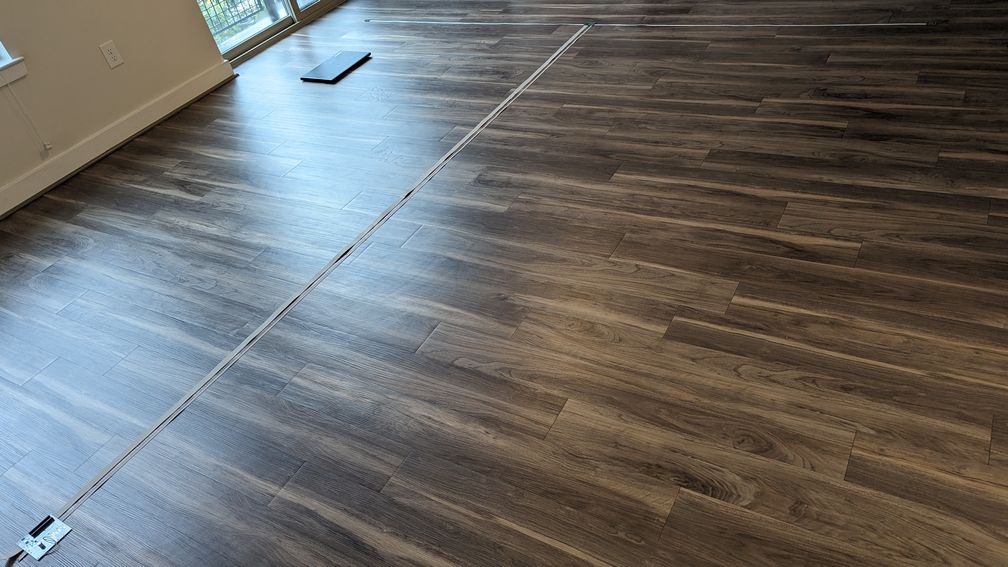
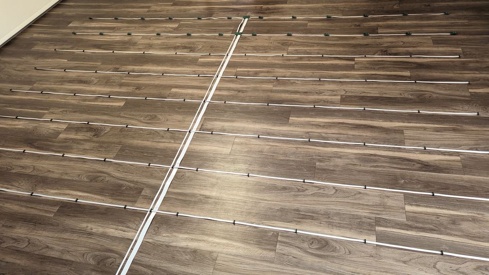
All 96 microphones in the 12 ft by 8 ft array are laid out for testing. A single ethernet wire connects the receiver board to a PoE switch, providing power to the microphone array and basic control functionality. Microphone data is saved to an SD card for subsequent processing.
The design worked as expected; the LVDS signaling allowed for error-free synchronization and data transmission continuously over multiple minutes (I did not carry out a test to run this until desynchronization occurred, as I never needed to record more than a few minutes at a time, but I have seen the array remain synchronized to the 2.5 MHz BCLK for over 10 minutes). The FlexIO module worked well, once I figured out the best way to set it up, and it is the proper tool to use for data serialization like this. The buffers and routines associated with moving data between buffers were shown to be successful in handling normally encountered SD card delays (some 100 ms) while regularly reading in new audio data. Having eight parallel buses made for a good match to the eight shift registers of the FlexIO module. The PoE was also effective, and the power requirements of the microphone array were well under budget: 0.16 A idle, 0.78 A standby, and 1.06 A in full operation, compared to 2.7 A design based on the maximum datasheet specifications of the MLVDS chips. I expected the current consumption to be lower because the datasheet maximum will not apply to all devices, and particularly for the MLVDS chips this value was specified at up to 250 MHz clock which is 100 times higher than BCLK used here.
The microphones output 18 bits of data, and all 18 bits were recorded (for each group of 8 microphones, the extra 2 bits are placed adjacently so that 16-bit divisions are maintained). Control of the recording functionality over ethernet with a simple html document served by the Teensy 4.1 was demonstrated. Having recorded some audio data, I soon ran into the question of what to do with it. The audio data is passed through a high-pass filter to remove the microphones' DC offset and allow for meaningful combination of multiple microphones' streams. The concentration of acoustic energy in 3D space could be calculated either by adding up waveforms in the time domain with a position-dependent time shift, or more confusingly by adding up the results of FFT transforms with position-dependent and frequency-dependent phase shifts (gfai tech's Knowledge Base website presents an overview of these approaches). The former is relatively easy to implement but has no frequency sensitivity and a basic implementation is limited to time shift steps that are discretized to the sample rate, which is a relatively coarse phase shift for high frequencies. The latter is slightly more difficult to implement and more computationally intensive, but has frequency and phase sensitivity (which could be used to generate color images) and is more robust in handling the discrete samples because it senses the presence of a sinusoid spread over many samples. I attempted to implement these methods in matlab and the script files (with some bonus FFT routines) may be downloaded here.
An ongoing challenge with this project is finding a suitable installation location. I have laid out the array in my studio apartment, which can be used for some rudimentary testing, but really this should be set up on a wall or hanging overhead in a large auditorium or concert hall. Until I get an opportunity to install this in a venue and record interesting audio data, I don't feel much inspiration to continue working on the data analysis side. With some matlab scripts, I was able to generate the following images, which seem to be related to physical locations of nearby sound sources.
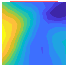
A 2D heatmap processed using addition of time-shifted audio signals from the microphones to back-project onto potential sources within the evaluated plane. The red rectangle in the upper half of the image shows the array location, and the heatmap is a slice about 1 meter above the array. The yellow regions towards the left of the image correspond to higher sound levels, apparently originating from the slightly open window to the left of the real array (the window may be seen in the layout photos above). The blue regions towards the upper right of the image correspond to lower sound levels, apparently coinciding with an open door to a closet from which sound is not well reflected.


2D heatmaps of FFT magnitudes at two different times within the recording processed using addition of phase-shifted FFT complex amplitudes to back-project onto potential sources within the evaluated plane. In playback with higher frame rate, the image changes rapidly and multiple times per second, on the scale of the wave period (the visualization could be compared to a high speed camera). The frequency shown is 250 Hz, with wavelength of about 4 ft, and some structure of similar dimensions is seen in the heatmap. Perhaps this is a room-scale resonance from a song that was playing in the background.
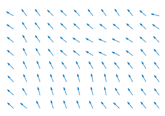

2D phase plots at two different times (unrelated to the magnitudes heatmap shown above) within the recording processed with FFT. The phase is shown as arrows rotated from theta=0 (pointing to right) by the phase of the added microphones' FFT complex amplitudes at each calculated location. There are times when the phase is largely uniform (left image) and other times when the phase fluctuates (right image). In playback with higher frame rate, the image changes rapidly on the scale of the wave period.
I came across a video on weighing an airplane based on a slight pressure rise underneath it as it is flying, and it made me curious whether I could see a pressure wave using the AFC microphone array when throwing a paper airplane (or some other object) over it. (See also my airplane pressure article which shows a successful measurement.) This breathed a bit of life back into the project and I made a few improvements to the firmware. The main limitation of the multiplexing design I used was that sampling would always be below the Nyquist frequency, meaning that frequency aliasing would occur. I assume that the microphones have built-in digital filters to remove frequency content above their sample rate Nyquist frequency, or about 20 kHz at microphone sample rate 40 kHz (unfortunately this was not specified on the datasheet; sometimes the cutoff frequency is lower). However I only read out 1 sample in 4 from each microphone, which in this example would be 10 kHz array sample rate and Nyquist frequency of 5 kHz, thus everything from 5 kHz to 20 kHz would be aliased into the data. The design was made with the hope that there would be relatively small amplitudes in that high frequency range, and the aliasing wouldn't matter, which I think has worked out fairly well. However a better choice would have been to use an asynchronous FIFO or a low-power Complex Programmable Logic Device, along with a fast bus clock around 40 MHz, to transfer every sample to the main board, after which digital filtering and decimation could have been used to lower the data rate without risk of aliasing.
Without making such large modifications, the scheme could still be slightly improved by raising the sample rate, because the amplitudes of higher frequencies are expected to be increasingly lower. The maximum supported clock for the microphones was 4 MHz or sample rate of 62.5 kHz (although it is likely they would work at higher clock rate, this blog post showed a similar microphone functioning with BCLK from 1024 kHz to 11264 kHz). Then the aliasing onset is raised to about 7.8 kHz. Increasing the bit clock was straightforward with a few changes in the firmware FlexIO clock divider and timer initialization lines. The differential signaling and microphones worked as expected, but the SD card could not keep up with the data rate. This uncovered a few bugs in the data processing code, such as that upon over-filling the buffer the interrupt flag would not get cleared (as normally it is cleared by reading the FlexIO shift registers) and then the interrupt would be called continuously, stalling the data acquisition altogether. With this fixed, I also added a data format description in the code so I can more easily remember it in the future, and slightly changed the way data is presented by the http server so that elapsed acquisition time is visible after acquisition is stopped. Another change is in the start-up of the microphone array; previously the clock was output for a few ms with the counters reset, which would present many clock pulses at the microphone without the expected LRCLK signal which was locally generated by the counters. This also relied on the reset line acting quickly to set the synchronization instant, while the reset line is not a differential circuit unlike BCLK. In the new startup, the reset line is pulsed on and off to initialize all the counters, and then the BCLK is connected at the proper moment to establish synchronization. This seems to work well and has the advantage of not dropping the first few ms of microphone output data (this data is not usable for sound measurement since the microphone is starting up, but allows confirmation of the microphone presence and functionality). It is possible to select 2.5 MHz or 4 MHz bit clock, and to enable or disable stop on synchronization error (the disable mode is useful when testing a partial array).
The latest firmware may be downloaded here. While the firmware works (except for a strange synchronization issue on my last recording attempt), the paper airplane experiment was not as successful. In the recording from the array I could hear the sound of the paper airplane being released and the "whoosh" that followed it, but there appeared to be no pressure rise discernible that would match the time scale of the paper airplane flying over the array. When the paper airplane flew into the wall by the array, the sound of the impact could be seen to travel from one end of the array to the other, at the speed of sound as expected (which was about 100 samples at 9765 Hz array sample rate). It was preceded by a faster component which was attributed to the seismic wave of the impact traveling through the floor (with expected ~10 times faster speed of sound). The lack of a clear pressure increase as the airplane flew over the array could be attributed to two factors. First the microphones are designed with an equalizing hole that acts as a high-pass filter with roll-off somewhere around 20 Hz. The airplane may have caused a perturbation at 1 Hz or lower, for which the sensitivity is reduced accordingly. Second the array length of 11 ft is not enough to guarantee that steady flight was established. Perhaps the airplane was in a largely parabolic (free-fall) trajectory while over the array in which case no pressure increase under it is to be expected. I attempted throwing the plane from farther away but again did not notice a difference. I also tried throwing a frisbee disc over the array, but it was even more difficult to throw the disc in a non-parabolic trajectory because it was designed for lift at higher speeds than I can achieve throwing it in the room where the array was set up, and I did not measure a pressure rise from the disc. Still it was interesting to revisit this project and maybe sometime I'll find another use for it.
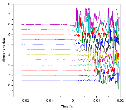
A plot of data from 12 microphones set up in a row, curves separated vertically for easier interpretation, with a frisbee disc thrown to fly over the microphones and crashing into a wall afterwards. There is no discernible pressure rise due to the disc flying, however upon hitting the wall the impulse is captured by the microphones. The top curve is the microphone closest to the impact location, and spacing between microphones is 1 ft. Note the fast seismic wave reaching the bottom microphone at around 2.5 ms, followed by the slower and higher amplitude sound wave reaching the bottom microphone at around 11 ms.