I have been experimenting with acquiring ECG and EEG data with the OpenBCI Cyton board, which has the ADS1299 bio-signal ADC and the PIC32MX250F128B microcontroller operating at 40 MHz. The firmware that is shipped with the board seems to work, but I wanted to add some improvements in the data processing and transmission capabilities, as well as expose all the configuration registers of the ADS1299 for computer control. The result is the MaxBCI firmware in C and associated PC software in C#. The features this firmware adds are:
This firmware also removes some functionality present in the OpenBCI version:
The Cyton board's main limitation is the radio communication to the computer. This is achieved using an RFduino radio, with its own firmware, and my firmware functions with the existing radio stack. The radio communication speed over the air is decent, allowing for 250 32-byte packets to be sent per second, or 64 kbit/s, which is well below maximum capability of the bluetooth protocol but it's enough that the effort to improve this isn't really justified. A big problem timing-wise however is the writing of data from the PIC32 to the radio buffer. With the baud rate of 115200, this process takes as long as 2.6 ms, where a 250 Hz packet rate means we have only 4 ms total, leaving 1.4 ms to do everything else. Reading in the data from the ADS1299, on the other hand, with an 8 MHz SPI bus, takes only 0.06 ms. So, with the way the radio is implemented, it is not possible to have any higher data sampling rate than 250 Hz, because at a higher rate like 2 kHz, just writing data to the radio will take up the time (2.6 ms) when about 5 new data packets should have been read in, because new data now arrives every 0.5 ms. In the existing firmware all this data is lost, and I'm really not sure how they claim to support these high data rates. The SD card does not fare much better - in between sectors, it has writing delays as long as 131 ms, which completely disrupts the continuous data flow from the ADS1299, and once again I have no idea how the original firmware claims to do this in a functional manner.
My firmware does support rates up to 2 kHz, by interleaving the data read-in calls with the radio send-out calls, sampling new data every 0.33 ms, and thus getting the latest data despite the embarrasingly slow radio serial bus implementation. However the radio output limitation of 32 bytes and 250 packets per second still applies. How can we convert 2 kHz into 250 Hz? This is done by altering the data stream, so that 8 sequential measurements at 2 kHz get sent together in 1 simultaneous packet of 8 data points at 250 Hz. This of course means that while the board can output 8 unique channels sampled at 250 Hz, it can only output 1 unique channel sampled at 2 kHz. As far as the computer receiving the data is concerned, both of these cases arrive in an identical format of 8 samples every 4 ms. My firmware handles the possibility of over-sampling or even under-sampling by defining a channel sequence, which is 16 entries long, and which determines what physical pins are sampled in each data packet. For example the typical channel sequence would be 1234567812345678, thus 8 unique channels (1 to 8) are sampled in each outgoing packet, and this is used with a data rate of 250 Hz. Alternatively, I could set a data rate of 2 kHz, and then set the channel sequence to 4444444444444444, which means only channel 4 is sampled, but it is sampled at 2 kHz instead of 250 Hz. Or, I could set a data rate of 500 Hz, with a channel sequence 1234123412341234, which means channels 1 to 4 will be sampled at 500 Hz.
Implementing this functionality was a fun exercise, because there are lots of intertwined bits of code that have to complete at the appropriate time and use up an appropriate duration of time, in order to properly handle time-division between reading in, parsing, and sending out the data. At the 2 kHz data rate, there are only about 1000 free CPU cycles between working code segments, or 0.025 ms, so the timing is not quite at the PIC32's limit but close to it. The firmware is capable of outputting 8 channels at 2 kHz, or maybe even faster, if a faster radio is used - which may be achievable with the WiFi shield, or at least that is the claim on the Cyton documentation. My firmware does not attempt this, but it should not be a difficult modification. Squeezing this performance out of the included bluetooth module was much trickier. This required a double-buffered approach on the data, and a new packet format to compress auxiliary data into just 4 bits per packet (thus the auxiliary 8-byte array is sent at 16 Hz, carried by the underlying main data stream at 250 Hz). The rest of the code handles data alignment and sequence order concerns.
Another feature implemented here is forward error correction. The packets are 32 bytes long on a hardware basis, but the ADS1299 only has eight unique channels resulting in 24 bytes. Along with header and footer bytes in the packet, this leaves 7 free bytes. The decision here was to use 6 of these bytes for a SECDED implementation with 26 data bytes and 5 code bytes and 1 total parity byte. The remaining 1 byte would be a combined auxiliary data byte and packet counter, used to ensure correct packet order and transmit 8 auxiliary data bytes at 16 Hz. The auxiliary data byte array includes the lead-off bytes for N and P sides on both base and daisy boards, the GPIO status, and the accelerometer readings. In the new packet format, bytes 0-23 carry the ADS1299 data, according to the channel sequence order. Byte 24 is the packet counter and aux data byte. Bytes 25-30 are the error correction bytes. If you don't care about error correction, bytes 25-30 can just be ignored. If you want a simple error check, calculate the XOR of bytes 0-29 and that should equal byte 30 if the packet is correct. If you want the complete error correction, it will be necessary to calculate the 5 Hamming parity bytes and compare them to bytes 25-29, and an example routine is given in the PC code below. The footer, byte 31, is 0xC1.
However using 6 bytes for error correction might be overkill, especially when we could use those 6 bytes to transmit another 2 channels of data. Thus my firmware implements a 10 channel mode, where the first 10 channels in the sequence are sampled at 250 Hz, and then the packet consists mostly of data. To use this mode a daisy board should be connected, which adds a second ADS1299 for a choice of 16 channels to sample (of which only the 10 appearing in the sequence will be sent by radio). In this packet format, bytes 0-29 are the 10 channels, and byte 30 is the combined packet counter and aux data carrier. The footer, byte 31, is 0xC8. There is no error protection in this case.
Additional functionality in the firmware is regarding the auxiliary hardware. It is possible to set up whether the onboard LED should be on or off during measurements, to turn the accelerometer on or off, and to allow the onboard PROG button to stop data transmission. This last point is useful because at high data rates the radio is so tasked that it usually misses any requests from the computer and thus the data transmission cannot be stopped once it is started.
The main code for the MaxBCI firmware can be downloaded here as a .ino file for the Arduino GUI. Compiling this also requires a modified BoardDefs header available here. The code files for the PC software can be downloaded here as a zip folder containing visual studio C# project files.
To load the firmware onto the Cyton board, you can follow the guides on the OpenBCI programming page. This involves adding the OpenBCI board in the Arduino interface, and then holding down the PROG button while turning on the board. The PIC32 can then be programmed over radio at a transmission rate that brings back memories of dial-up internet. The Cyton board should now have the new firmware, indicated with the blinking LED and a status message over the serial link reading out MaxBCI v1.0. There should be no need to modify the radio firmware.
For the PC software, you will need Visual Studio 2017 or later, then you can import the C# project and compile. For the plots, I use SciChart, which requires a license, so those files won't compile. I would suggest using the core functionality of the packet handling, which is implemented in the InterfaceBCISerial class, and copying that into your own application. ControlBCI is a GUI that enables most of the MaxBCI commands to be sent to the board. The code in MainWindow demonstrates a way to have multiple listener classes in the list BCIListeners, which can all handle the data in different ways: ControlPlotter plots multiple channels, ControlFFT plots an FFT spectrum of a channel, and SleepTracker carries out sleep study analysis.
This is the data packet as received by the PC from Cyton over the RFduino dongle. The output from the board is designed so that a data processor can safely continuously listen for 0xA0 as it will only be returned in advance of a data packet. As mentioned above, the firmware supports two modes, 8-channel and 10-channel, which have slightly differing formats.
1 Header byte 0xA0
24 byte channel values = 8 readings, channel number based on loaded sequence and data rate, confirmed in packet number counter
1 byte 0xYZ where Y is the packet counter which increments from 0 to F (15) for each sent packet, for tracking losses due to radio transmission
	and for figuring out what channel sequence this packet is (0 for even, 8 for odd), and for figuring out what Z is.
	Z is used to transmit 8 aux bytes over 16 packets, where Z is the 4 bytes of the array
	[LOFF_STATP_BASE, LOFF_STATN_BASE, LOFF_STATP_DAISY, LOFF_STATN_DAISY, GPIO, ACC_X_H, ACC_Y_H, ACC_Z_H] sent sequentially (MSB first)
5 bytes error correction parity (Hamming code, assuming D26=0x00)
1 byte data parity (XOR of the previous 30 bytes)
1 Footer byte 0xC1
1 Header byte 0xA0
30 byte channel values = 10 readings, channel numbers are steps 1-10 in sequence
1 byte 0xYZ where Y is the packet counter which increments from 0 to F (15) for each sent packet, for tracking losses due to radio transmission
	and for figuring out what Z is.
	Z is used to transmit 8 aux bytes over 16 packets, where Z is the 4 bytes of the array
	[LOFF_STATP_BASE, LOFF_STATN_BASE, LOFF_STATP_DAISY, LOFF_STATN_DAISY, GPIO, ACC_X_H, ACC_Y_H, ACC_Z_H] sent sequentially (MSB first)
1 Footer byte 0xC8
These commands are sent from PC to Cyton over the RFduino dongle. Commands must be preceded with a semicolon ":" and ended with an \r\n line break. Commands are a single capital letter followed by some constant number of parameters. Only the commands D and V result in a response, otherwise there is no response but the onboard LED will flash rapidly if the command is received (and the board is not streaming).
Q Set up channel sequence
	Does not write anything to ADS registers, only internal processing
	Followed by 16 valid characters
	The board will convert channels in sequence. This allows use of higher sampling rates with fewer active channels. Sequence length is 16.
	Channels for the base board are 12345678 and for daisy are 9:;<=>?@ (which are the ASCII characters after 8)
	Default sequence is 1234567812345678 if daisy not connected at power-up, and 123456789:;<=>?@ if daisy is connected at power-up
	Example :Q1234567812345678\r\n, transmitted chars = 20
B Set up bias generator properties
	Writes BIAS_SENSP and BIAS_SENSN registers on board and also daisy if connected
	Default is nothing connected (all 0)
	Followed by 16 characters (each per channel) to determine bias generation connection (if daisy not connected, the last 8 don't matter but still must be sent):
		n = n side only
		p = p side only
		1 = both n and p sides connected to bias generation
		0 = nothing connected to bias generation
	Example :B0000111100000000\r\n, transmitted chars = 20
R Set up data acquisition rate
	Writes to CONFIG1[DR] (when implemented)
	Followed by a letter value which can be
		a =250 Hz, b = 500 Hz, c =1000 Hz, d =2000 Hz all in 8-channel mode; A = 250 Hz in 10-channel mode
		Which means that every data-ready event the number of channels loaded from sequence per step is 8, 4, 2, 1, 10 respectively
	Default is 250 Hz. Rate is always the same for both base and daisy boards.
	Packets are always sent back at 250 Hz, so selecting a higher sample rate is only useful
	with a repetitive channel sequence (Q command) for over-sampling
	Example :Ra\r\n, transmitted chars = 5
S Start coninuous data conversion and transmission to PC
F Finish continuous data conversion and transmission to PC
	Start or End command affects both board and daisy ADS
	Example :S\r\n, transmitted chars = 4
V Report firmware and protocol version, also hardware IDs and status
D Get a print output of debug variables and counters (such as min/max write times)
	Example :D\r\n, transmitted chars = 4
C Set up channel input properties
	Writes to CHnSET on board or daisy depending on channel number
	Followed by channel ID, which is 1-8 for base board and 9-@ for daisy
	Followed by mode
		0=off
		i=input
		s=shorted
		b=bias measure (must set corresponding enable bit with P command)
		m=MVDD
		t=temperature
		c=calibration (test) signal
		p=bias output on P
		n=bias output on N
	Followed by SRB2
		0 or 1
	Followed by gain
		1 =1, 2 =2, 4 =4, 6 =6, 8 =8, c =12, o =24
	Default is all powered on and shorted and 24x gain and SRB2 off
	Each channel is set up individually and independently, command must be issued for each channel at start up
	Example :C1i01\r\n, transmitted chars = 8
P Set up board-wide properties
	Writes CONFIG3[BIAS_MEAS], MISC1[SRB1], CONFIG4[PD_LOFF_COMP]
	Default 000
	Followed by base or daisy selection or all
		b=base
		d=daisy
		a=all
	Followed by BIAS meas enable (0/1), SRB1 enable (0/1), lead-off comparator enable (0/1)
	Example :Pa000\r\n, transmitted chars = 8
O Set up lead-off channel connection
	Writes LOFF_SENSP, LOFF_SENSN, LOFF_FLIP, Selects either board or daisy based on channel number except for turning off writes 0 to both
	Default 0000
	Followed by channel for positive current selection followed by 'p' or 'n', then channel for negative current selection followed by 'p' or 'n'
		Note lead-off N will not connect to SRB1 bus if it is used, but lead-off P will connect to SRB2 if the corresponding channel is connected!
		Refer to datasheet Fig 18
		For the SRB1 situation, can use flipped lead-off to connect N excitation source to an otherwise P electrode
		The flipped lead-off calculation is done automatically on specification of p and n in above command, for instance
		1p1n will not be flipped while 1n1p will be
	Or 0000 to turn off lead-off registers on both boards
	Example :O1p1n\r\n, O0000\r\n, transmitted chars = 8
L Set up lead-off signal properties
	Writes LOFF register
	Default 000
	Followed by base or daisy selection or all
		b=base
		d=daisy
		a=all
	Followed by mode: DC or AC frequency, and current amplitude, and comparator threshold
		0=dc, 1=ac 7.8Hz, 2=ac 31.2 Hz, 3=ac f_DR/4 (62.5 Hz at 250 data rate)
		0=6 nA, 1=24 nA, 2=6 uA, 3=24 uA
		0-7 corresponding to 95%-70% threshold, per Table 16 in datasheet, this is only useful when P command is used to enable lead-off
		comparators and only on channels configured for lead off by the O command
	Example :La000\r\n, transmitted chars = 8
T Set up test signal properties
	Writes CONFIG2 register
	Defaults are 00
	Followed by base or daisy selection or all
		b=base
		d=daisy
		a=all
	Followed by oscillating signal freq+ampl
		0=dc, 1=0.975 Hz, 2=1.95 Hz
		0=1.875 mV, 1=3.75 mV  (given as zero-peak (dc mode), pk-pk (ac mode) is twice this = 3.75mV and 7.5mV)
		Connect it to a channel for measurement by using the C command
	Example :Ta10\r\n, transmitted chars = 7
A Turn accessories on or off
	Defaults are 1111
	Followed by LED on/off, accelerometer on/off, LEADOFF output on/off, GPIO output on/off+stop on PROG (defaults are on for all)
		0=LED off during stream, 1=LED on during stream (led always blinks in idle state / when stream is off), 2 & 3=LED is used as input
		during stream (pin D11) with pull-up off or on respectively
		0=accelerometer off during stream (sent bytes are undefined), 1=accelerometer on during stream and sent interleaved in packets
		on aux bytes 5-7
		0=lead off output bytes are not sent during stream (if GPIO is enabled, it will be sent on both bytes 0 and 4), 1=lead off output bytes
		from both base and daisy are sent interleaved in packets on aux bytes 0-3
		0=GPIO status is not sent during stream (sent byte is undefined) and stop on PROG (D17), 1=onboard GPIO status sent during stream
		interleaved in packets on aux byte 4 and stop on PROG (D17), 2=no GPIO and no stop on PROG, 3 = GPIO and no stop on PROG
	Example :A0000\r\n, transmitted chars = 8
E Set up error correction mode (for 8ch mode only)
	Default is 1
	Followed by error mode type
		0=bytes 25-30 not set, 1=bytes 25-30 are Hamming correction and parity, 2=high speed GPIO data on bytes 25-29 and total parity on byte 30
	Example :E1\r\n, transmitted chars = 5
There are a few electrode configurations that can be usefully measured with this board and firmware. While the Cyton board is at least nominally meant to support EEG measurements, I haven't gotten useful EEG data out of it, the results are very noisy and can barely be interpreted. This is due to both the dry electrodes not having good skin contact and the board itself being completely open to electrical interference as it is unshielded and ungrounded. In theory the ADS1299 should have sufficient sensitivity to do EEG measurements, and maybe this can be done with sufficient patience. However I've mostly used this board for ECG and muscle measurements, where the signals are much stronger and wet electrodes much easier to apply. The electrodes make a huge difference, as does proper bias setup and grounding. Also it is important to avoid any loops of wires (or virtual loops), as these act like antennas and pick up lots of noise; instead ensure all wires are twisted together so they follow one path. Better yet would be to use shielded cables, but as the board itself is not shielded this probably won't make as much of an impact.
This configuration allows for very simple heart rate and rapid eye movement detection, which can be useful in a sleep study. Here 2 electrodes are connected on either side of the chest to measure heart rate, and 2 electrodes are connected on the sides of the head by each eye to measure eye motion. On the ADS1299, the REM electrodes are connected to the N and P pins of channel 4, and the HR electrodes are connected to the N and P pins of channel 3 (any other channels numbers can be used, 3 and 4 are arbitrary). Both of these are configured for x24 amplification, and N bias output is turned on for the HR channel. The bias generator is set to use the N and P sides of the REM channel, and the P side of the HR channel. Channel 5 is set up as a temperature sensor, and the accelerometer readings are also recorded.
In the resulting data, the heart rate will appear as sharp pulses on the HR channel, and eye movement will appear as large increases in the frequency range 0.25 - 3.0 Hz which can be extracted by Fourier analysis. The following plot shows a measurement of heart rate and REM over a few hours using the above setup.
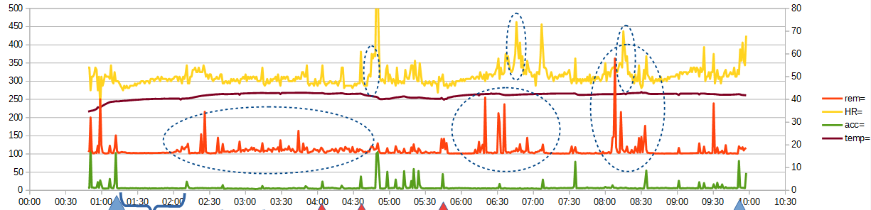
A sleep study with HR, REM, temperature, and accelerometer measurements. Note the initial deep sleep period followed by the onset of REM, with regular positional changes and a rise in temperature. There are 3 distinguishable REM periods outlined in the plot. Typically increased HR tends to end the REM periods, and increased motion occurs about 4 hours after sleep onset once the first REM cycle is done.
The medical terminology associated with ECG is confusing from an electrical engineering standpoint, because the 3-lead ECG only requires 2 voltage measurements from a common reference. In fact there can be as many as 6 "leads" all made from these 2 measurements, by adding and subtracting them in different manners. These are called the three standard leads and three augmented leads. The information carried is the same, just displayed a bit differently.
Electrode 1 is placed by the right arm (RA). Electrode 2 is placed by the left arm (LA). Electrode 3 is placed by the left leg (LL). Electrode 4 is placed by the right leg (RL). RL is used for bias only and is not measured. RA is the common reference point, and LA with LL provide the two unique voltages. We can then define V1 = LA-RA, and V2 = LL-RA. Now for the medical terminology:
| Lead | Formula | Voltage |
|---|---|---|
| I | LA-RA | V1 |
| II | LL-RA | V2 |
| III | II-I = LL-LA | V2-V1 |
| aVR | -(I+III/2) = RA-(LA+LL)/2 | (V1+V2)/-2 |
| aVL | I-II/2 = LA-(LL+RA)/2 | V1-V2/2 |
| aVF | II-I/2 = LL-(LA+RA)/2 | V2-V1/2 |
On the Cyton board, this configuration can be implemented by using the SRB1 functionality. Connect the 4 electrodes as, LA and LL to P pins of channels 1 and 2, RA to the SRB1 pin, RL to bias pin. Then enable SRB1, thus placing a virtual jumper that connects all N pins together, and in particular RA to the N pins on both channels. Configure the bias generator to be based on the P pins of both channels, and the channels for x24 amplification. The data on the computer will be V1 in channel 1, and V2 in channel 2. The rest of the 6 leads can be computed with the above formulas. The following plot shows an ECG measurement with the above setup.
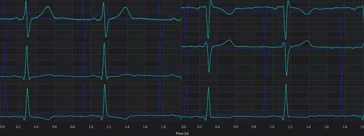
A 6-lead ECG plot generated with the new firmware and PC software. The image is a combination of multiple plots, so the Y scales are not identical between the plots (unlike a standard ECG printout), but the X scales are. The PR interval is approximately 0.12 s, QRS is 0.08 s. The axis is approaching 90 degrees.
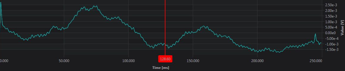
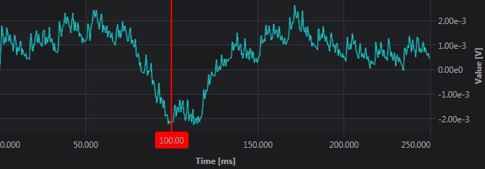
The ADS1299 has an internal oscillator at 0.975 Hz or 1.95 Hz, which can be used to test the board without needing an external signal generator. This is quite simple - configure the channel to be tested as test mode (c) using the C command, then set up the test signal generator using the T command. The measured outputs of that channel should give the correct amplitude and frequency. Also temperature and chip voltage can be measured (though not battery voltage, another hardware oversight). The following plot is an example with the 0.95 Hz test waveform and temperature:
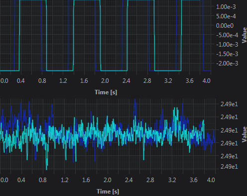
The first channel is outputting a 0.975 Hz test waveform of pk-pk amplitude 3.75 mV, while the second is outputting the device temperature of 24.9 C.
The 2 kHz sample rate, along with fast GPIO sampling (also at 2 kHz), allows for decent quality evoked potential data, where the EEG waveform is synchronized to a signal like a strobe or a click by using the GPIO as an indicator of the stimulus initiation time. However the wiring as a whole is noisy, and it is very difficult to remove the noise: neither the cables nor the board are shielded or designed with noise immunity in mind. I attempted measuring visual evoked potentials with flash and pattern reversal stimuli, using GPIO18 to synchronize the measurement to the stimulus. The following plots show approximately 400 measurements averaged:
Flash VEP
Pattern Reversal VEP

Checkerboard pattern projected on wall for pattern reversal VEP, and state of pattern was measured with a photodiode to synchronize ECG data acquisition to moment of pattern change
Both the 8 channel mode and the 10 channel mode are working correctly, at all data rates. The daisy module functions as intended when the channel sequence is modified to include it. All the configuration options are also working properly. The accelerometer output is correct, as is the GPIO functionality, and all commands. Overall I would call this project a success.
The biggest issues with the board include the inability to actually output 8 channels at 2 kHz despite being able to read it in (the ADS1299 can go up to 16 kHz, which this board won't even approach) due to the slow radio, and the poor shielding design which makes the inputs very susceptible to noise. I would say this board can be used for hobby level exploration and quick home measurements, but it is not sufficiently robust for research grade applications.
Practically, the benefit of the forward error correction in the sent out packets has been small. While identified uncorrectable packets were about 0.084% of all received, identified correctable packets were only 0.014%. So effectively the same performance can be achieved by just throwing out any packets that don't pass the total parity check instead of bothering to correct them, but maybe this conclusion will differ in other environments with different types of radio interference. Still there is the increased confidence benefit that the packets which do pass the parity checks are much more likely to be unaltered. Overall 99.8% to 99.9% of the packets are correctly received, tested over a period of more than 10 hours continuous operation. The ones that aren't received or are uncorrectable, seem to appear in bursts of faulty data affecting up to 10 packets in a row, whereas outside these bursts the reception is flawless, so the noise or interference is not constant but periodic, perhaps due to nearby radio devices like cell phones and WiFi transmitters.
As for the onboard reading and transmission of data, from the ADS1299 to the radio, the reliability and timing has been a perfect 100% at all data rates. The following is a test report of the onboard timing parameters at the different data rates. Note the consistent 0 missed packets, indicating that all the data from the ADS1299 has been processed and sent out on time. Also note the free cycles decreasing and output time increasing as the data rate goes up, as well as the almost doubled read time in the 10 channel mode (since this requests data from 2 ADS chips instead of the usual 1). The ratio of received to sent packets also goes up at higher data rates, due to the over-sampling, so at 2 kHz there are 8 packets received for each 1 packet sent (with the excess data ignored).
DR = 250 (4ms between DRs, 1.9ms between packets)
	Min free cycles = 403
	Missed packets = 0
	Ontime packets = 356
	Recd packets = 356
	Sent packets = 356
	Read max time = 46
	Output max time = 2027
DR=500 (2ms between DRs, 1.1ms between packet internals)
	Min free cycles = 191
	Missed packets = 0
	Ontime packets = 1476
	Recd packets = 1476
	Sent packets = 738
	Read max time = 51
	Output max time = 2074
DR=1000 (1ms between DRs, 0.91ms between packet internals)
	Min free cycles = 195
	Missed packets = 0
	Ontime packets = 2399
	Recd packets = 2399
	Sent packets = 599
	Read max time = 46
	Output max time = 2510
DR=2000 (0.5ms between DRs, 0.41ms between packet internals)
	Min free cycles = 90
	Missed packets = 0
	Ontime packets = 5452
	Recd packets = 5452
	Sent packets = 681
	Read max time = 51
	Output max time = 2590
DR=250 in 10ch mode (4ms between DRs, 1.8ms between packets)
	Min free cycles = 256
	Missed packets = 0
	Ontime packets = 861
	Recd packets = 861
	Sent packets = 861
	Read max time = 92
	Output max time = 2120